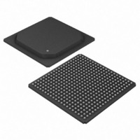
DS3163 Maxim Integrated Products, DS3163 Datasheet - Page 305

DS3163
Manufacturer Part Number
DS3163
Description
IC TRPL ATM/PACKET PHY 400-PBGA
Manufacturer
Maxim Integrated Products
Datasheet
1.DS3163.pdf
(384 pages)
Specifications of DS3163
Applications
*
Mounting Type
Surface Mount
Package / Case
400-BGA
Lead Free Status / RoHS Status
Lead free / RoHS Compliant
Available stocks
Company
Part Number
Manufacturer
Quantity
Price
- Current page: 305 of 384
- Download datasheet (4Mb)
12.12 DS3/E3 PLCP
12.12.1 Transmit Side PLCP
The transmit side utilizes seven registers.
12.12.1.1 Register Map
Table 12-43. Transmit Side PLCP Register Map
12.12.1.2 Register Bit Descriptions
Register Name:
Register Description:
Register Address:
Bit #
Name
Default
Bit #
Name
Default
Bits 4 to 3: Transmit M2 and M1 Byte Control (TMC[1:0]) – These two bits control the source of the transmit M2
and M1 bytes.
Bits 2 to 1: Transmit F1 Byte Control (TF1C[1:0]) – These two bits control the source of the transmit F1 byte.
Note: If TMC[1:0] is 00 and TF1C[1:0] is 01, the F1 byte will be invalid. If TMC[1:0] is 01 and TF1C[1:0] is 01, both
M2 and F1 will carry the transmit HDLC data link. If TMC[1:0] is 10 and TF1C[1:0] is 01, both M1 and F1 will carry
the transmit HDLC data link. When F1 and M# both carry the transmit HDLC data link, the F1 byte and M# byte in
the same frame may or may not be equal.
Bit 0: Automatic REI Defeat (AREID) – When 0, the REI is automatically generated based upon the parity (BIP-8)
errors detected in the receive PLCP Frame Processor. When 1, the REI is inserted from the G1 register bits
TREI[3:0].
(1,3,5,7)5Ch
(1,3,5,7)5Ah
(1,3,5,7)5Eh
(1,3,5,7)50h
(1,3,5,7)52h
(1,3,5,7)54h
(1,3,5,7)56h
(1,3,5,7)58h
Address
00 = concatenated M1 and M2 (128 kHz) from transmit HDLC controller.
01 = M2 (64 kHz) from transmit HDLC controller; M1 from M1 byte register (PLCP.TM12BR).
10 = M2 from M2 byte register; M1 (64 kHz) from transmit HDLC controller.
11 = M2 from M2 byte register; M1 from M1 byte register
00 = transmit Trail Trace controller.
01 = transmit HDLC controller.
10 = F1 byte register (PLCP.TFGBR).
11 = reserved
15
--
--
0
7
0
PLCP.TM12BR
PLCP.TZ12BR
PLCP.TZ34BR
PLCP.TZ56BR
PLCP.TFGBR
PLCP.TEIR
PLCP.TCR
Register
--
14
--
--
0
6
0
PLCP.TCR
PLCP Transmit Control Register
(1,3,5,7)50h
PLCP Transmit Control Register
PLCP Transmit Error Insertion Register
PLCP Transmit F1 and G1 Byte Register
PLCP Transmit M1 and M2 Byte Register
PLCP Transmit Z1 and Z2 Byte Register
PLCP Transmit Z3 and Z4 Byte Register
PLCP Transmit Z5 and Z6 Byte Register
Unused
13
--
--
0
5
0
Register Description
TMC1
12
--
0
0
4
TMC0
11
--
0
3
0
TF1C1
10
--
0
2
0
TF1C0
--
9
0
1
0
AREID
--
8
0
0
0
Related parts for DS3163
Image
Part Number
Description
Manufacturer
Datasheet
Request
R

Part Number:
Description:
MAX7528KCWPMaxim Integrated Products [CMOS Dual 8-Bit Buffered Multiplying DACs]
Manufacturer:
Maxim Integrated Products
Datasheet:

Part Number:
Description:
Single +5V, fully integrated, 1.25Gbps laser diode driver.
Manufacturer:
Maxim Integrated Products
Datasheet:

Part Number:
Description:
Single +5V, fully integrated, 155Mbps laser diode driver.
Manufacturer:
Maxim Integrated Products
Datasheet:

Part Number:
Description:
VRD11/VRD10, K8 Rev F 2/3/4-Phase PWM Controllers with Integrated Dual MOSFET Drivers
Manufacturer:
Maxim Integrated Products
Datasheet:

Part Number:
Description:
Highly Integrated Level 2 SMBus Battery Chargers
Manufacturer:
Maxim Integrated Products
Datasheet:

Part Number:
Description:
Current Monitor and Accumulator with Integrated Sense Resistor; ; Temperature Range: -40°C to +85°C
Manufacturer:
Maxim Integrated Products

Part Number:
Description:
TSSOP 14/A�/RS-485 Transceivers with Integrated 100O/120O Termination Resis
Manufacturer:
Maxim Integrated Products

Part Number:
Description:
TSSOP 14/A�/RS-485 Transceivers with Integrated 100O/120O Termination Resis
Manufacturer:
Maxim Integrated Products

Part Number:
Description:
QFN 16/A�/AC-DC and DC-DC Peak-Current-Mode Converters with Integrated Step
Manufacturer:
Maxim Integrated Products

Part Number:
Description:
TDFN/A/65V, 1A, 600KHZ, SYNCHRONOUS STEP-DOWN REGULATOR WITH INTEGRATED SWI
Manufacturer:
Maxim Integrated Products

Part Number:
Description:
Integrated Temperature Controller f
Manufacturer:
Maxim Integrated Products

Part Number:
Description:
SOT23-6/I�/45MHz to 650MHz, Integrated IF VCOs with Differential Output
Manufacturer:
Maxim Integrated Products

Part Number:
Description:
SOT23-6/I�/45MHz to 650MHz, Integrated IF VCOs with Differential Output
Manufacturer:
Maxim Integrated Products

Part Number:
Description:
EVALUATION KIT/2.4GHZ TO 2.5GHZ 802.11G/B RF TRANSCEIVER WITH INTEGRATED PA
Manufacturer:
Maxim Integrated Products

Part Number:
Description:
QFN/E/DUAL PCIE/SATA HIGH SPEED SWITCH WITH INTEGRATED BIAS RESISTOR
Manufacturer:
Maxim Integrated Products
Datasheet:


