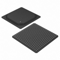
DS3163 Maxim Integrated Products, DS3163 Datasheet - Page 44

DS3163
Manufacturer Part Number
DS3163
Description
IC TRPL ATM/PACKET PHY 400-PBGA
Manufacturer
Maxim Integrated Products
Datasheet
1.DS3163.pdf
(384 pages)
Specifications of DS3163
Applications
*
Mounting Type
Surface Mount
Package / Case
400-BGA
Lead Free Status / RoHS Status
Lead free / RoHS Compliant
Available stocks
Company
Part Number
Manufacturer
Quantity
Price
- Current page: 44 of 384
- Download datasheet (4Mb)
8.2 Detailed Pin Descriptions
Table 8-2. Detailed Pin Descriptions
n = 1,2,3,4 (port number); Ipu (input with pullup); Oz (output tri-stateable, needs an external pullup or pulldown resistor to keep from floating);
Oa (analog output); Ia (analog input); I/O (bidirectional inout); all unused input pins without pullup should be tied low.
TPOSn /
TLCLKn
TDATn
PIN
TYPE
O
O
Transmit Line Clock Output
TLCLKn: This clock is typically used as the clock reference for the TPOSn / TDATn
and TNEG / TOHMOn signals, but can also be used as the reference for the TOHMIn
/ TSOFIn, TFOHn / TSERn, TFOHENIn and TSOFOn / TDENn / TFOHENOn signals.
This output signal can be inverted.
o
o
o
Transmit Positive AMI / Data Output
TPOSn: When the port line interface is configured for B3ZS, HDB3 or AMI mode and
the framer is not configured for one of the “-OHM” modes (see
on this pin indicates that a positive pulse should be transmitted on the line. The signal
is updated on the positive clock edge of the referenced clock pin if the clock pin signal
is not inverted, otherwise it is updated on the falling edge of the clock. The signal is
typically referenced to the TLCLKn line clock output pins, but it can be referenced to
the TCLKOn, TCLKIn, RLCLKn or RCLKOn pins.
This output signal can be inverted.
TDATn: When the port line interface is configured for UNI mode or the framer is
configured for one of the “-OHM” modes (see
signal is output on this pin. The signal is updated on the positive clock edge of the
referenced clock pin if the clock pin signal is not inverted, otherwise it is updated on
the falling edge of the clock. The signal is typically referenced to the TLCLK line clock
output pins, but it can be referenced to the TCLKOn, TCLKIn, RLCLKn or RCLKOn
pins
This output signal can be inverted.
o
o
o
DS3: 44.736 MHz +20 ppm
E3: 34.368 MHz +20 ppm
CC52: 52 MHz +20 ppm
DS3: 44.736 Mbps +20ppm
E3: 34.368 Mbps +20ppm
CC52: 52 Mbps +20ppm
LINE I/O
FUNCTION
Table
10-30), the un-encoded transmit
Table
10-30), a high
Related parts for DS3163
Image
Part Number
Description
Manufacturer
Datasheet
Request
R

Part Number:
Description:
MAX7528KCWPMaxim Integrated Products [CMOS Dual 8-Bit Buffered Multiplying DACs]
Manufacturer:
Maxim Integrated Products
Datasheet:

Part Number:
Description:
Single +5V, fully integrated, 1.25Gbps laser diode driver.
Manufacturer:
Maxim Integrated Products
Datasheet:

Part Number:
Description:
Single +5V, fully integrated, 155Mbps laser diode driver.
Manufacturer:
Maxim Integrated Products
Datasheet:

Part Number:
Description:
VRD11/VRD10, K8 Rev F 2/3/4-Phase PWM Controllers with Integrated Dual MOSFET Drivers
Manufacturer:
Maxim Integrated Products
Datasheet:

Part Number:
Description:
Highly Integrated Level 2 SMBus Battery Chargers
Manufacturer:
Maxim Integrated Products
Datasheet:

Part Number:
Description:
Current Monitor and Accumulator with Integrated Sense Resistor; ; Temperature Range: -40°C to +85°C
Manufacturer:
Maxim Integrated Products

Part Number:
Description:
TSSOP 14/A�/RS-485 Transceivers with Integrated 100O/120O Termination Resis
Manufacturer:
Maxim Integrated Products

Part Number:
Description:
TSSOP 14/A�/RS-485 Transceivers with Integrated 100O/120O Termination Resis
Manufacturer:
Maxim Integrated Products

Part Number:
Description:
QFN 16/A�/AC-DC and DC-DC Peak-Current-Mode Converters with Integrated Step
Manufacturer:
Maxim Integrated Products

Part Number:
Description:
TDFN/A/65V, 1A, 600KHZ, SYNCHRONOUS STEP-DOWN REGULATOR WITH INTEGRATED SWI
Manufacturer:
Maxim Integrated Products

Part Number:
Description:
Integrated Temperature Controller f
Manufacturer:
Maxim Integrated Products

Part Number:
Description:
SOT23-6/I�/45MHz to 650MHz, Integrated IF VCOs with Differential Output
Manufacturer:
Maxim Integrated Products

Part Number:
Description:
SOT23-6/I�/45MHz to 650MHz, Integrated IF VCOs with Differential Output
Manufacturer:
Maxim Integrated Products

Part Number:
Description:
EVALUATION KIT/2.4GHZ TO 2.5GHZ 802.11G/B RF TRANSCEIVER WITH INTEGRATED PA
Manufacturer:
Maxim Integrated Products

Part Number:
Description:
QFN/E/DUAL PCIE/SATA HIGH SPEED SWITCH WITH INTEGRATED BIAS RESISTOR
Manufacturer:
Maxim Integrated Products
Datasheet:


