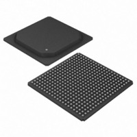
DS3163 Maxim Integrated Products, DS3163 Datasheet - Page 230

DS3163
Manufacturer Part Number
DS3163
Description
IC TRPL ATM/PACKET PHY 400-PBGA
Manufacturer
Maxim Integrated Products
Datasheet
1.DS3163.pdf
(384 pages)
Specifications of DS3163
Applications
*
Mounting Type
Surface Mount
Package / Case
400-BGA
Lead Free Status / RoHS Status
Lead free / RoHS Compliant
Available stocks
Company
Part Number
Manufacturer
Quantity
Price
- Current page: 230 of 384
- Download datasheet (4Mb)
Bit 4: Loop Time Enable (LOOPT). When this bit is set, the port is in loop time mode. The transmit clock is set to
the receive clock from the RLCLKn pin or the recovered clock from the CLAD clock and the TCLKIn pin is not used.
This function of this bit is conditional on other control bits. See
Bit 3: CLAD Transmit Clock Source Control (CLADC). This bit is used to enable the CLAD clocks as the
source of the internal transmit clock. This function of this bit is conditional on other control bits. See
more details.
Bit 2: Receive Framer IO Signal Timing Select (RFTS). This bit controls the timing reference for the signals on
the receive framer interface IO pins. The pins controlled are RSERn, RSOFOn / RDENn / RFOHENn and
RFOHENn. See
Bit 1: Transmit Framer IO Signal Timing Select (TFTS). This bit controls the timing reference for the signals on
the transmit framer interface IO pins. The pins controlled are TOHMIn / TSOFIn, TFOHn / TSERn, TFOHENIn and
TSOFOn / TDENn / TFOHENOn. See
Bit 0: Transmit Line IO Signal Timing Select (TLTS). This bit controls the timing reference for the signals on the
transmit line interface IO pins. The pins controlled are TPOSn / TDATn and TNEGn / TOHMOn. See
more details.
Register Name:
Register Description:
Register Address:
Bit #
Name
Default
Bit #
Name
Default
Bit 11: System Bus Loopback (SLB). This bit enables the system bus loopback mode per port when the bit is
set. ATM cells and/or HDLC packets are looped back from the transmit system bus to the receive system bus
through the FIFOs. See
Bits 10 to 8: Loopback Mode [2:0] (LBM[2:0]). These bits select the loopback modes for analog loopback (ALB),
line loopback (LLB), payload loopback (PLB) and diagnostic loopback (DLB). See
select codes. Default: No Loopback.
LBM[2:0]
10X
000
001
010
011
110
0 = Normal transmit clock operation
1 = Transmit using the receive clock
0 = Use CLAD clocks for the transmit clock as appropriate
1 = Do not use CLAD clocks for the transmit clock – (if no loopback is enabled, TCLKIn is the source)
0 = Use output clocks for timing reference
1 = Use input clocks for timing reference
0 = Use output clocks for timing reference
1 = Use input clocks for timing reference
0 = Use output clocks for timing reference
1 = Use input clocks for timing reference
GPIOB3
15
--
0
7
0
Table 10-7
ALB
0
1
0
0
0
0
Figure 10-9
GPIOB2
for more details.
14
--
0
6
0
LLB
0
0
1
0
0
1
PORT.CR4
Port Control Register 4
(0,2,4,6)46h
for the block diagram highlighting loopback features.
PLB
Table 10-6
GPIOB1
0
0
0
1
0
0
13
--
0
5
0
DLB
0
0
0
0
1
1
for more details.
GPIOB0
12
--
0
0
4
Table 10-3
GPIOA3
SLB
11
0
3
0
for more details.
GPIOA2
LBM2
10
0
2
0
Table 10-15
GPIOA1
LBM1
9
0
1
0
for the loopback
Table 10-3
Table 10-5
GPIOA0
LBM0
8
0
0
0
for
for
Related parts for DS3163
Image
Part Number
Description
Manufacturer
Datasheet
Request
R

Part Number:
Description:
MAX7528KCWPMaxim Integrated Products [CMOS Dual 8-Bit Buffered Multiplying DACs]
Manufacturer:
Maxim Integrated Products
Datasheet:

Part Number:
Description:
Single +5V, fully integrated, 1.25Gbps laser diode driver.
Manufacturer:
Maxim Integrated Products
Datasheet:

Part Number:
Description:
Single +5V, fully integrated, 155Mbps laser diode driver.
Manufacturer:
Maxim Integrated Products
Datasheet:

Part Number:
Description:
VRD11/VRD10, K8 Rev F 2/3/4-Phase PWM Controllers with Integrated Dual MOSFET Drivers
Manufacturer:
Maxim Integrated Products
Datasheet:

Part Number:
Description:
Highly Integrated Level 2 SMBus Battery Chargers
Manufacturer:
Maxim Integrated Products
Datasheet:

Part Number:
Description:
Current Monitor and Accumulator with Integrated Sense Resistor; ; Temperature Range: -40°C to +85°C
Manufacturer:
Maxim Integrated Products

Part Number:
Description:
TSSOP 14/A�/RS-485 Transceivers with Integrated 100O/120O Termination Resis
Manufacturer:
Maxim Integrated Products

Part Number:
Description:
TSSOP 14/A�/RS-485 Transceivers with Integrated 100O/120O Termination Resis
Manufacturer:
Maxim Integrated Products

Part Number:
Description:
QFN 16/A�/AC-DC and DC-DC Peak-Current-Mode Converters with Integrated Step
Manufacturer:
Maxim Integrated Products

Part Number:
Description:
TDFN/A/65V, 1A, 600KHZ, SYNCHRONOUS STEP-DOWN REGULATOR WITH INTEGRATED SWI
Manufacturer:
Maxim Integrated Products

Part Number:
Description:
Integrated Temperature Controller f
Manufacturer:
Maxim Integrated Products

Part Number:
Description:
SOT23-6/I�/45MHz to 650MHz, Integrated IF VCOs with Differential Output
Manufacturer:
Maxim Integrated Products

Part Number:
Description:
SOT23-6/I�/45MHz to 650MHz, Integrated IF VCOs with Differential Output
Manufacturer:
Maxim Integrated Products

Part Number:
Description:
EVALUATION KIT/2.4GHZ TO 2.5GHZ 802.11G/B RF TRANSCEIVER WITH INTEGRATED PA
Manufacturer:
Maxim Integrated Products

Part Number:
Description:
QFN/E/DUAL PCIE/SATA HIGH SPEED SWITCH WITH INTEGRATED BIAS RESISTOR
Manufacturer:
Maxim Integrated Products
Datasheet:


