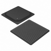
DS3163 Maxim Integrated Products, DS3163 Datasheet - Page 16

DS3163
Manufacturer Part Number
DS3163
Description
IC TRPL ATM/PACKET PHY 400-PBGA
Manufacturer
Maxim Integrated Products
Datasheet
1.DS3163.pdf
(384 pages)
Specifications of DS3163
Applications
*
Mounting Type
Surface Mount
Package / Case
400-BGA
Lead Free Status / RoHS Status
Lead free / RoHS Compliant
Available stocks
Company
Part Number
Manufacturer
Quantity
Price
- Current page: 16 of 384
- Download datasheet (4Mb)
3 FEATURE DETAILS
The following sections describe the features provided by the DS3161 (single), DS3162 (dual), DS3163 (triple), and
DS3164 (quad) PHYs.
•
•
•
•
•
•
•
•
•
•
•
•
•
•
•
•
•
•
•
•
•
•
•
•
•
3.1 Global Features
•
•
Each port independently configurable
Universal PHYs map ATM cells and/or HDLC packets into DS3 or E3 data streams
UTOPIA L2/L3 or POS-PHY L2/L3 OR SPI-3 interface with 8-, 16-, or 32-bit bus
66MHz UTOPIA L3 and POS-PHY L3 clock
52MHz UTOPIA L2 and POS-PHY L2 clock
Ports independently configurable for cell or packet traffic in POS-PHY bus modes
Direct, PLCP, DSS, and clear-channel cell mapping
Direct and clear-channel packet mapping
On-chip DS3 (M23 or C-bit) and E3 (G.751 or G.832) framer(s)
Ports independently configurable for DS3, E3 (full or sub-rate) or arbitrary framing protocols up to 52 Mbps
Programmable (externally controlled or internally finite state machine controlled) subrate DS3/E3
Full featured DS3/E3/PLCP alarm generation and detection
Built-in HDLC controllers with 256-byte FIFOs for the insertion/extraction of DS3 PMDL, G.751 Sn bit and
G.832 NR/GC bytes, and PLCP NR/GC bytes
On-chip BERTs for PRBS and repetitive pattern generation, detection, and analysis
Large performance-monitoring counters for accumulation intervals of at least 1 second
Flexible overhead insertion/extraction ports for DS3, E3, and PLCP framers
Loopbacks include line, diagnostic, framer, payload, terminal, and system interface with capabilities to insert
AIS in the directions away from loopback directions
Ports can be disabled to reduce power
Integrated Clock Rate Adapter to generate the remaining internally required 44.736MHz (DS3), 34.368MHz
(E3), and 52MHz (arbitrary framing at up to 52 Mbps) from a single clock reference source at one of those
three frequencies
Pin and Software Compatible with DS3181–DS3184 Single–Quad ATM/Packet PHYs with Built-In LIUs and
DS3171–DS3174 Single–Quad DS3/E3 Single-Chip Transceivers—Framers and LIUs
8/16-bit generic microprocessor interface
Low power (1.6W typ) 3.3V operation (5V tolerant I/O)
Small high-density thermally enhanced BGA packaging (TE-PBGA) with 1.27mm pin pitch
Industrial temperature operation: -40°C to 85°C
IEEE1149.1 JTAG test port
System interface configurable for UTOPIA L2 / UTOPIA L3 for ATM cell traffic or POS-PHY L2 / POS-PHY L3
or SPI-3 for HDLC packets or mixed packet/cell traffic
Supports the following transmission protocols:
•
•
•
•
•
•
•
•
•
•
•
•
Direct-mapped ATM over DS3 or sub-rate DS3
PLCP-mapped ATM over DS3
Direct-mapped ATM over G.751 E3 or sub-rate G.751 E3
PLCP-mapped ATM over G.751 E3
Direct-mapped ATM over G.832 E3 or sub-rate G.832 E3
Bit or byte synchronous (octet-aligned) direct-mapped ATM over externally-defined frame formats up to
52 Mbps
Clear-channel ATM (cell-based physical layer) at line rates up to 52 Mbps
Clear-channel ATM DSS at line rates up to 52 Mbps
Direct-mapped HDLC over DS3 or sub-rate DS3
Direct-mapped HDLC over G.751 E3 or sub-rate G.751 E3
Direct-mapped HDLC over G.832 E3 or sub-rate G.832 E3
Bit or byte synchronous (octet-aligned) direct-mapped HDLC over externally-defined frame formats up
to 52 Mbps
Related parts for DS3163
Image
Part Number
Description
Manufacturer
Datasheet
Request
R

Part Number:
Description:
MAX7528KCWPMaxim Integrated Products [CMOS Dual 8-Bit Buffered Multiplying DACs]
Manufacturer:
Maxim Integrated Products
Datasheet:

Part Number:
Description:
Single +5V, fully integrated, 1.25Gbps laser diode driver.
Manufacturer:
Maxim Integrated Products
Datasheet:

Part Number:
Description:
Single +5V, fully integrated, 155Mbps laser diode driver.
Manufacturer:
Maxim Integrated Products
Datasheet:

Part Number:
Description:
VRD11/VRD10, K8 Rev F 2/3/4-Phase PWM Controllers with Integrated Dual MOSFET Drivers
Manufacturer:
Maxim Integrated Products
Datasheet:

Part Number:
Description:
Highly Integrated Level 2 SMBus Battery Chargers
Manufacturer:
Maxim Integrated Products
Datasheet:

Part Number:
Description:
Current Monitor and Accumulator with Integrated Sense Resistor; ; Temperature Range: -40°C to +85°C
Manufacturer:
Maxim Integrated Products

Part Number:
Description:
TSSOP 14/A�/RS-485 Transceivers with Integrated 100O/120O Termination Resis
Manufacturer:
Maxim Integrated Products

Part Number:
Description:
TSSOP 14/A�/RS-485 Transceivers with Integrated 100O/120O Termination Resis
Manufacturer:
Maxim Integrated Products

Part Number:
Description:
QFN 16/A�/AC-DC and DC-DC Peak-Current-Mode Converters with Integrated Step
Manufacturer:
Maxim Integrated Products

Part Number:
Description:
TDFN/A/65V, 1A, 600KHZ, SYNCHRONOUS STEP-DOWN REGULATOR WITH INTEGRATED SWI
Manufacturer:
Maxim Integrated Products

Part Number:
Description:
Integrated Temperature Controller f
Manufacturer:
Maxim Integrated Products

Part Number:
Description:
SOT23-6/I�/45MHz to 650MHz, Integrated IF VCOs with Differential Output
Manufacturer:
Maxim Integrated Products

Part Number:
Description:
SOT23-6/I�/45MHz to 650MHz, Integrated IF VCOs with Differential Output
Manufacturer:
Maxim Integrated Products

Part Number:
Description:
EVALUATION KIT/2.4GHZ TO 2.5GHZ 802.11G/B RF TRANSCEIVER WITH INTEGRATED PA
Manufacturer:
Maxim Integrated Products

Part Number:
Description:
QFN/E/DUAL PCIE/SATA HIGH SPEED SWITCH WITH INTEGRATED BIAS RESISTOR
Manufacturer:
Maxim Integrated Products
Datasheet:


