DS3163 Maxim Integrated Products, DS3163 Datasheet - Page 77

DS3163
Manufacturer Part Number
DS3163
Description
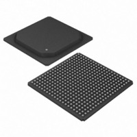
IC TRPL ATM/PACKET PHY 400-PBGA
Manufacturer
Maxim Integrated Products
Datasheet
1.DS3163.pdf
(384 pages)
Specifications of DS3163
Applications
*
Mounting Type
Surface Mount
Package / Case
400-BGA
Lead Free Status / RoHS Status
Lead free / RoHS Compliant
Available stocks
Company
Part Number
Manufacturer
Quantity
Price
- Current page: 77 of 384
- Download datasheet (4Mb)
Figure 8-31
the ATM device polls PHY port 'N'. On clock edge 3, PHY port 'N' indicates to the ATM device that it can accept cell
data by asserting TPXA. On clock edge 5, the ATM device selects PHY port 'N'. On clock edge 6, the ATM device
starts a cell transfer to PHY port 'N' by asserting TEN, placing the first byte of cell data on TDATA, and asserting
TSOX to indicate the transfer of the first byte of the cell. On clock edge 7, the ATM device de-asserts TSOX as it
continues to place additional bytes of the cell on TDATA. On clock edge 11, the ATM device polls PHY port 'M'. On
clock edge 12, the ATM device polls PHY port 'N'. On clock edge 13, PHY port 'M' indicates that it can accept the
transfer of a complete cell. On clock edge 14, PHY port 'N' indicates that it cannot accept the transfer of a complete
cell. On clock edge 16, the ATM device deselects PHY port 'N' and selects PHY port 'M' by de-asserting TEN and
placing PHY port 'M's address on TADR. On clock edge 17, the ATM device starts the transfer of a cell to PHY port
'M' by asserting TEN, placing the first byte of cell data on TDATA, and asserting TSOX to indicate the transfer of
the first byte of the cell. On clock edge 18, the ATM device de-asserts TSOX as it continues to place additional
bytes of the cell on TDATA.
Figure 8-31. UTOPIA Level 3 Transmit Multiple Cell Transfer Polled Mode
Transfer
TDATA
Cell To:
TADR
TSOX
TCLK
TPXA
TEN
M
K
X
shows a multi-port transmit interface multiple cell transfer to different PHY devices. On clock edge 1,
1
N
L
X
2
O
M
X
3
N
P
X
4
Q
O
X
5
N
P
X
6
H1
Q
R
7
H2
X
J
8
H3
K
R
9
…
…
…
10
N
P43
L
J
11
P44
M
K
12
P45
N
L
13
P46
M
O
14
P47
P
N
15
P48
Q
O
16
M
P
X
17
H1
R
Q
18
M
H2
X
J
19
H3
R
K
20
P1
L
J
Related parts for DS3163
Image
Part Number
Description
Manufacturer
Datasheet
Request
R

Part Number:
Description:
MAX7528KCWPMaxim Integrated Products [CMOS Dual 8-Bit Buffered Multiplying DACs]
Manufacturer:
Maxim Integrated Products
Datasheet:

Part Number:
Description:
Single +5V, fully integrated, 1.25Gbps laser diode driver.
Manufacturer:
Maxim Integrated Products
Datasheet:

Part Number:
Description:
Single +5V, fully integrated, 155Mbps laser diode driver.
Manufacturer:
Maxim Integrated Products
Datasheet:

Part Number:
Description:
VRD11/VRD10, K8 Rev F 2/3/4-Phase PWM Controllers with Integrated Dual MOSFET Drivers
Manufacturer:
Maxim Integrated Products
Datasheet:

Part Number:
Description:
Highly Integrated Level 2 SMBus Battery Chargers
Manufacturer:
Maxim Integrated Products
Datasheet:

Part Number:
Description:
Current Monitor and Accumulator with Integrated Sense Resistor; ; Temperature Range: -40°C to +85°C
Manufacturer:
Maxim Integrated Products

Part Number:
Description:
TSSOP 14/A�/RS-485 Transceivers with Integrated 100O/120O Termination Resis
Manufacturer:
Maxim Integrated Products

Part Number:
Description:
TSSOP 14/A�/RS-485 Transceivers with Integrated 100O/120O Termination Resis
Manufacturer:
Maxim Integrated Products

Part Number:
Description:
QFN 16/A�/AC-DC and DC-DC Peak-Current-Mode Converters with Integrated Step
Manufacturer:
Maxim Integrated Products

Part Number:
Description:
TDFN/A/65V, 1A, 600KHZ, SYNCHRONOUS STEP-DOWN REGULATOR WITH INTEGRATED SWI
Manufacturer:
Maxim Integrated Products

Part Number:
Description:
Integrated Temperature Controller f
Manufacturer:
Maxim Integrated Products

Part Number:
Description:
SOT23-6/I�/45MHz to 650MHz, Integrated IF VCOs with Differential Output
Manufacturer:
Maxim Integrated Products

Part Number:
Description:
SOT23-6/I�/45MHz to 650MHz, Integrated IF VCOs with Differential Output
Manufacturer:
Maxim Integrated Products

Part Number:
Description:
EVALUATION KIT/2.4GHZ TO 2.5GHZ 802.11G/B RF TRANSCEIVER WITH INTEGRATED PA
Manufacturer:
Maxim Integrated Products

Part Number:
Description:
QFN/E/DUAL PCIE/SATA HIGH SPEED SWITCH WITH INTEGRATED BIAS RESISTOR
Manufacturer:
Maxim Integrated Products
Datasheet:


