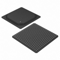
DS3163 Maxim Integrated Products, DS3163 Datasheet - Page 309

DS3163
Manufacturer Part Number
DS3163
Description
IC TRPL ATM/PACKET PHY 400-PBGA
Manufacturer
Maxim Integrated Products
Datasheet
1.DS3163.pdf
(384 pages)
Specifications of DS3163
Applications
*
Mounting Type
Surface Mount
Package / Case
400-BGA
Lead Free Status / RoHS Status
Lead free / RoHS Compliant
Available stocks
Company
Part Number
Manufacturer
Quantity
Price
- Current page: 309 of 384
- Download datasheet (4Mb)
12.12.2 Receive Side PLCP Register Map
The receive side utilizes thirteen registers.
Table 12-44. Receive Side PLCP Register Map
12.12.2.1 Register Bit Descriptions
Register Name:
Register Description:
Register Address:
Bit #
Name
Default
Bit #
Name
Default
Bits 9 to 8: Receive HDLC Source Control (RHSC[1:0]) – These two bits control the source of the receive HDLC
controller.
Bit 6: Receive LOF Integration Enable (RLIE) – When 0, the receive Loss Of Frame (LOF) integration counter is
disabled. When 1, the receive LOF integration counter is enabled.
Bit 4: Parity Error Count Control (PECC) – When 0, BIP-8 (B1 byte) bit errors are detected (up to 8 per frame).
When 1, BIP-8 block errors are detected (no more than one per frame). Note: The transmit REI bits are affected by
the setting of this bit as the REI bits reflect the number of BIP-8 errors detected/counted.
Bit 3: Framing Error POI Disable (FEPD) – When 0, Path Overhead Indicator (POI) byte (P#) and framing
alignment byte (A1 & A2) errors are detected. When 1, only A1 & A2 errors are detected. Note: This bit is ignored
when OOF events are counted (FECC=1)
Bit 2: Framing Error Count Control (FECC) – This bit controls the type of framing error events that are counted.
When 0, A1 byte errors, A2 byte errors, and P# byte errors (up to 3 per subframe) are counted. When 1, OOF
events are counted.
(1,3,5,7)6Ch
(1,3,5,7)7Ch
(1,3,5,7)6Ah
(1,3,5,7)6Eh
(1,3,5,7)7Ah
(1,3,5,7)7Eh
(1,3,5,7)60h
(1,3,5,7)62h
(1,3,5,7)64h
(1,3,5,7)66h
(1,3,5,7)68h
(1,3,5,7)70h
(1,3,5,7)72h
(1,3,5,7)74h
(1,3,5,7)76h
(1,3,5,7)78h
Address
00 = F1 byte.
01 = M1 byte.
10 = M2 byte.
11 = M2 and M1 byte.
15
--
--
0
7
0
PLCP.RM12BR
PLCP.RZ12BR
PLCP.RZ34BR
PLCP.RZ56BR
PLCP.RSRIE1
PLCP.RSRIE2
PLCP.RPECR
PLCP.RPECR
PLCP.RFGBR
PLCP.RFECR
PLCP.RSRL1
PLCP.RSRL2
PLCP.RSR1
PLCP.RSR2
PLCP.RCR
Register
--
RLIE
14
--
0
6
0
PLCP.RCR
PLCP Receive Control Register
(1,3,5,7)60h
PLCP Receive Control Register
Unused
PLCP Receive Status Register #1
PLCP Receive Status Register #2
PLCP Receive Status Register Latched #1
PLCP Receive Status Register Latched #2
PLCP Receive Status Register Interrupt Enable #1
PLCP Receive Status Register Interrupt Enable #2
PLCP Receive Framing Error Count Register
PLCP Receive P-bit Parity Error Count Register
PLCP Receive REI Error Count Register
PLCP Receive F1 and G1 Byte Register
PLCP Receive M1 and M2 Byte Register
PLCP Receive Z1 and Z2 Byte Register
PLCP Receive Z3 and Z4 Byte Register
PLCP Receive Z5 and Z6 Byte Register
13
--
--
0
5
0
PECC
12
Register Description
--
0
0
4
FEPD
11
--
0
3
0
FECC
10
--
0
2
0
RHSC1
ECC
9
0
1
0
FRSYNC
RHSC0
8
0
0
0
Related parts for DS3163
Image
Part Number
Description
Manufacturer
Datasheet
Request
R

Part Number:
Description:
MAX7528KCWPMaxim Integrated Products [CMOS Dual 8-Bit Buffered Multiplying DACs]
Manufacturer:
Maxim Integrated Products
Datasheet:

Part Number:
Description:
Single +5V, fully integrated, 1.25Gbps laser diode driver.
Manufacturer:
Maxim Integrated Products
Datasheet:

Part Number:
Description:
Single +5V, fully integrated, 155Mbps laser diode driver.
Manufacturer:
Maxim Integrated Products
Datasheet:

Part Number:
Description:
VRD11/VRD10, K8 Rev F 2/3/4-Phase PWM Controllers with Integrated Dual MOSFET Drivers
Manufacturer:
Maxim Integrated Products
Datasheet:

Part Number:
Description:
Highly Integrated Level 2 SMBus Battery Chargers
Manufacturer:
Maxim Integrated Products
Datasheet:

Part Number:
Description:
Current Monitor and Accumulator with Integrated Sense Resistor; ; Temperature Range: -40°C to +85°C
Manufacturer:
Maxim Integrated Products

Part Number:
Description:
TSSOP 14/A�/RS-485 Transceivers with Integrated 100O/120O Termination Resis
Manufacturer:
Maxim Integrated Products

Part Number:
Description:
TSSOP 14/A�/RS-485 Transceivers with Integrated 100O/120O Termination Resis
Manufacturer:
Maxim Integrated Products

Part Number:
Description:
QFN 16/A�/AC-DC and DC-DC Peak-Current-Mode Converters with Integrated Step
Manufacturer:
Maxim Integrated Products

Part Number:
Description:
TDFN/A/65V, 1A, 600KHZ, SYNCHRONOUS STEP-DOWN REGULATOR WITH INTEGRATED SWI
Manufacturer:
Maxim Integrated Products

Part Number:
Description:
Integrated Temperature Controller f
Manufacturer:
Maxim Integrated Products

Part Number:
Description:
SOT23-6/I�/45MHz to 650MHz, Integrated IF VCOs with Differential Output
Manufacturer:
Maxim Integrated Products

Part Number:
Description:
SOT23-6/I�/45MHz to 650MHz, Integrated IF VCOs with Differential Output
Manufacturer:
Maxim Integrated Products

Part Number:
Description:
EVALUATION KIT/2.4GHZ TO 2.5GHZ 802.11G/B RF TRANSCEIVER WITH INTEGRATED PA
Manufacturer:
Maxim Integrated Products

Part Number:
Description:
QFN/E/DUAL PCIE/SATA HIGH SPEED SWITCH WITH INTEGRATED BIAS RESISTOR
Manufacturer:
Maxim Integrated Products
Datasheet:


