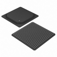
DS3163 Maxim Integrated Products, DS3163 Datasheet - Page 147

DS3163
Manufacturer Part Number
DS3163
Description
IC TRPL ATM/PACKET PHY 400-PBGA
Manufacturer
Maxim Integrated Products
Datasheet
1.DS3163.pdf
(384 pages)
Specifications of DS3163
Applications
*
Mounting Type
Surface Mount
Package / Case
400-BGA
Lead Free Status / RoHS Status
Lead free / RoHS Compliant
Available stocks
Company
Part Number
Manufacturer
Quantity
Price
- Current page: 147 of 384
- Download datasheet (4Mb)
DS3161/DS3162/DS3163/DS3164
10.8.3 Transmit PLCP Frame Processor
The Transmit PLCP Frame Processor receives the ATM cells from the ATM/Packet Processor performs trailer
generation, framing generation, error insertion, and overhead insertion.
The bits in a byte are transmitted MSB first, LSB last. When they are input serially, they are input in the order they
are to be transmitted. The bits in a byte in an outgoing signal are numbered in the order they are transmitted, 1
(MSB) to 8 (LSB). However, when a byte is stored in a register, the MSB is stored in the highest numbered bit (7),
and the LSB is stored in the lowest numbered bit (0). This is to differentiate between a byte in a register and the
corresponding byte in a signal.
10.8.4 Receive PLCP Frame Processor
The Receive PLCP Frame Processor accepts the data stream from the DS3/E3 Framer and extracts the entire
DS3/E3 overhead and processes only the PLCP frame data.
The bits in a byte are received MSB first, LSB last. When they are output serially, they are output in the order they
are received. The bits in a byte in an incoming signal are numbered in the order they are received, 1 (MSB) to 8
(LSB). However, when a byte is stored in a register, the MSB is stored in the highest numbered bit (7), and the LSB
is stored in the lowest numbered bit (0). This is to differentiate between a byte in a register and the corresponding
byte in a signal.
Some bits, bit groups, or bytes (data) are integrated. Integration requires the data to have a new value for five
consecutive occurrences before the new data value will be stored in the data register. Integrated data may have an
associated unstable indication. Integrated data is considered unstable if for eight consecutive occurrences the
received data value does not match the currently stored (integrated) data value or the previously received data
value.
10.8.5 Transmit DS3 PLCP Frame Processor
The DS3 PLCP frame format is shown in
Figure
10-30. A1 and A2 are the subframe alignment bytes that have a
value of F6h and 28h respectively. P11 – P0 are the Path Overhead Identifier (POI) bytes that indicate the path
overhead byte contained in the current subframe. Z6 – Z1 are growth bytes reserved for future use. F1 is the Path
User Channel byte allocated for user communications purposes (This byte is undefined in ATM). B1 is the Bit
Interleaved Parity-8 (BIP-8) byte used for PLCP path error monitoring. G1 is the PLCP Path Status Byte (See
Figure
10-31) used for far-end path status and performance monitoring (bits 6 – 8 are undefined in ATM). M2 and
M1 are the DQDB Layer Management Information bytes used for DQDB layer management communications
(These bytes are undefined in ATM). C1 is the Cycle/Stuff Counter byte used as for PLCP superframe alignment
and stuff indication.
Related parts for DS3163
Image
Part Number
Description
Manufacturer
Datasheet
Request
R

Part Number:
Description:
MAX7528KCWPMaxim Integrated Products [CMOS Dual 8-Bit Buffered Multiplying DACs]
Manufacturer:
Maxim Integrated Products
Datasheet:

Part Number:
Description:
Single +5V, fully integrated, 1.25Gbps laser diode driver.
Manufacturer:
Maxim Integrated Products
Datasheet:

Part Number:
Description:
Single +5V, fully integrated, 155Mbps laser diode driver.
Manufacturer:
Maxim Integrated Products
Datasheet:

Part Number:
Description:
VRD11/VRD10, K8 Rev F 2/3/4-Phase PWM Controllers with Integrated Dual MOSFET Drivers
Manufacturer:
Maxim Integrated Products
Datasheet:

Part Number:
Description:
Highly Integrated Level 2 SMBus Battery Chargers
Manufacturer:
Maxim Integrated Products
Datasheet:

Part Number:
Description:
Current Monitor and Accumulator with Integrated Sense Resistor; ; Temperature Range: -40°C to +85°C
Manufacturer:
Maxim Integrated Products

Part Number:
Description:
TSSOP 14/A�/RS-485 Transceivers with Integrated 100O/120O Termination Resis
Manufacturer:
Maxim Integrated Products

Part Number:
Description:
TSSOP 14/A�/RS-485 Transceivers with Integrated 100O/120O Termination Resis
Manufacturer:
Maxim Integrated Products

Part Number:
Description:
QFN 16/A�/AC-DC and DC-DC Peak-Current-Mode Converters with Integrated Step
Manufacturer:
Maxim Integrated Products

Part Number:
Description:
TDFN/A/65V, 1A, 600KHZ, SYNCHRONOUS STEP-DOWN REGULATOR WITH INTEGRATED SWI
Manufacturer:
Maxim Integrated Products

Part Number:
Description:
Integrated Temperature Controller f
Manufacturer:
Maxim Integrated Products

Part Number:
Description:
SOT23-6/I�/45MHz to 650MHz, Integrated IF VCOs with Differential Output
Manufacturer:
Maxim Integrated Products

Part Number:
Description:
SOT23-6/I�/45MHz to 650MHz, Integrated IF VCOs with Differential Output
Manufacturer:
Maxim Integrated Products

Part Number:
Description:
EVALUATION KIT/2.4GHZ TO 2.5GHZ 802.11G/B RF TRANSCEIVER WITH INTEGRATED PA
Manufacturer:
Maxim Integrated Products

Part Number:
Description:
QFN/E/DUAL PCIE/SATA HIGH SPEED SWITCH WITH INTEGRATED BIAS RESISTOR
Manufacturer:
Maxim Integrated Products
Datasheet:


