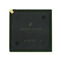
MPC561MZP56 Freescale, MPC561MZP56 Datasheet - Page 1059

MPC561MZP56
Manufacturer Part Number
MPC561MZP56
Description
Manufacturer
Freescale
Datasheet
1.MPC561MZP56.pdf
(1420 pages)
Specifications of MPC561MZP56
Cpu Family
MPC56x
Device Core
PowerPC
Device Core Size
32b
Frequency (max)
56MHz
Interface Type
QSPI/SCI/SPI/UART
Total Internal Ram Size
32KB
# I/os (max)
56
Number Of Timers - General Purpose
22
Operating Supply Voltage (typ)
2.6/5V
Operating Supply Voltage (max)
2.7/5.25V
Operating Supply Voltage (min)
2.5/4.75V
On-chip Adc
2(32-chx10-bit)
Instruction Set Architecture
RISC
Operating Temp Range
-40C to 125C
Operating Temperature Classification
Automotive
Mounting
Surface Mount
Pin Count
388
Package Type
BGA
Program Memory Type
ROMLess
Program Memory Size
Not Required
Lead Free Status / RoHS Status
Not Compliant
Available stocks
Company
Part Number
Manufacturer
Quantity
Price
Company:
Part Number:
MPC561MZP56
Manufacturer:
Freescale Semiconductor
Quantity:
10 000
Company:
Part Number:
MPC561MZP56R2
Manufacturer:
Freescale Semiconductor
Quantity:
10 000
- Current page: 1059 of 1420
- Download datasheet (11Mb)
The 520-bit boundary scan register can be connected between TDI and TDO by selecting the EXTEST or
SAMPLE/PRELOAD instructions. This register is used to capturing signal pin data on the input pins,
forcing fixed values on the output signal pins, and selecting the direction and drive characteristics (a logic
value or high impedance) of the bidirectional and three-state signal pins.
The key to using the boundary scan register is knowing the boundary scan bit order and the pins that are
associated with them.
input.
Table 25-1
bit definitions for the MPC563.
Freescale Semiconductor
BSDL
Bit
10
11
12
13
14
15
16
17
18
19
20
21
22
23
24
25
0
1
2
3
4
5
6
7
8
9
BC_2
BC_7
BC_2
BC_2
BC_2
BC_7
BC_2
BC_7
BC_2
BC_7
BC_2
BC_7
BC_2
BC_7
BC_2
BC_7
BC_2
BC_7
BC_2
BC_7
BC_2
BC_7
BC_2
BC_7
BC_2
BC_7
Type
displays boundary scan bit definitions for the MPC561 and
Cell
Table 25-1
Pin/Port Name
B_TPUCH10
B_TPUCH0
B_TPUCH1
B_TPUCH2
B_TPUCH3
B_TPUCH4
B_TPUCH5
B_TPUCH6
B_TPUCH7
B_TPUCH8
B_TPUCH9
B_CNRX0
B_CNTX0
Table 25-1. MPC561 Boundary Scan Bit Definition
*
*
*
*
*
*
*
*
*
*
*
*
*
MPC561/MPC563 Reference Manual, Rev. 1.2
shows the bit order starting from the TDO output and going to the TDI
Function
controlr
internal
output2
controlr
controlr
controlr
controlr
controlr
controlr
controlr
controlr
controlr
controlr
controlr
BSDL
bidir
bidir
bidir
bidir
bidir
bidir
bidir
bidir
bidir
bidir
bidir
bidir
Safe
Valu
e
0
0
1
1
0
0
0
0
0
0
0
0
0
0
0
0
0
0
0
0
0
0
0
0
0
0
Contro
Cell
10
12
14
16
18
20
22
24
0
4
6
8
l
Disable
Value
Table 25-2
0
0
0
0
0
0
0
0
0
0
0
0
IEEE 1149.1-Compliant Interface (JTAG)
Disable
Result
Z
Z
Z
Z
Z
Z
Z
Z
Z
Z
Z
Z
displays boundary scan
Function
Pin
IO
IO
IO
IO
IO
IO
IO
IO
IO
IO
IO
IO
O
Type
5vsa
5vsa
5vsa
5vsa
5vsa
5vsa
5vsa
5vsa
5vsa
5vsa
5vsa
Pad
5vfa
5vfa
25-5
Related parts for MPC561MZP56
Image
Part Number
Description
Manufacturer
Datasheet
Request
R

Part Number:
Description:
MPC5 1K0 5%
Manufacturer:
TE Connectivity
Datasheet:

Part Number:
Description:
MPC5 500R 5%
Manufacturer:
TE Connectivity
Datasheet:

Part Number:
Description:
MPC5 5K0 5%
Manufacturer:
Tyco Electronics
Datasheet:

Part Number:
Description:
MPC5 5R0 5%
Manufacturer:
Tyco Electronics
Datasheet:

Part Number:
Description:
MPC5 50K 5%
Manufacturer:
Tyco Electronics
Datasheet:

Part Number:
Description:
MPC5 1R0 5%
Manufacturer:
Tyco Electronics
Datasheet:

Part Number:
Description:
TOWER ELEVATOR BOARDS HARDWARE
Manufacturer:
Freescale Semiconductor
Datasheet:

Part Number:
Description:
TOWER SERIAL I/O HARDWARE
Manufacturer:
Freescale Semiconductor
Datasheet:

Part Number:
Description:
LCD MODULE FOR TWR SYSTEM
Manufacturer:
Freescale Semiconductor
Datasheet:

Part Number:
Description:
DAUGHTER LCD WVGA I.MX51
Manufacturer:
Freescale Semiconductor
Datasheet:

Part Number:
Description:
TOWER SYSTEM BOARD MPC5125
Manufacturer:
Freescale Semiconductor
Datasheet:


