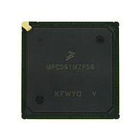
MPC561MZP56 Freescale, MPC561MZP56 Datasheet - Page 664

MPC561MZP56
Manufacturer Part Number
MPC561MZP56
Description
Manufacturer
Freescale
Datasheet
1.MPC561MZP56.pdf
(1420 pages)
Specifications of MPC561MZP56
Cpu Family
MPC56x
Device Core
PowerPC
Device Core Size
32b
Frequency (max)
56MHz
Interface Type
QSPI/SCI/SPI/UART
Total Internal Ram Size
32KB
# I/os (max)
56
Number Of Timers - General Purpose
22
Operating Supply Voltage (typ)
2.6/5V
Operating Supply Voltage (max)
2.7/5.25V
Operating Supply Voltage (min)
2.5/4.75V
On-chip Adc
2(32-chx10-bit)
Instruction Set Architecture
RISC
Operating Temp Range
-40C to 125C
Operating Temperature Classification
Automotive
Mounting
Surface Mount
Pin Count
388
Package Type
BGA
Program Memory Type
ROMLess
Program Memory Size
Not Required
Lead Free Status / RoHS Status
Not Compliant
Available stocks
Company
Part Number
Manufacturer
Quantity
Price
Company:
Part Number:
MPC561MZP56
Manufacturer:
Freescale Semiconductor
Quantity:
10 000
Company:
Part Number:
MPC561MZP56R2
Manufacturer:
Freescale Semiconductor
Quantity:
10 000
- Current page: 664 of 1420
- Download datasheet (11Mb)
Queued Serial Multi-Channel Module
*Reads access the RDRx; writes access the TDRx.
During SCIx initialization, two bits in the SCCxR1 should be written last: the transmitter enable (TE) and
receiver enable (RE) bits, which enable SCIx. Registers SCCxR0 and SCCxR1 should both be initialized
at the same time or before TE and RE are asserted. A single half-word write to SCCxR1 can be used to
initialize SCIx and enable the transmitter and receiver.
15.7.2
SCCxR0 contains the SCIx baud rate selection field and two bits controlling the clock source. The baud
rate must be set before the SCI is enabled. The CPU can read and write SCCxR0 at any time.
Changing the value of SCCxR0 bits during a transfer operation can disrupt the transfer. Before changing
register values, allow the SCI to complete the current transfer, then disable the receiver and transmitter.
15-46
SRESET
Bits
3:15
0
1
2
Field OTHR
Addr
SCI Control Register 0 (SCCxR0)
LNKBD
SCxBR
MSB
OTHR
Name
0
0
—
0x30 504C-6A
0x30 502C —
0x30 504A
LNKBD
This bit is reserved and should always be programmed to 0.
This bit is reserved and should always be programmed to 0.
Reserved
SCI baud rate. The SCI baud rate is programmed by writing a 13-bit value to this field. Writing a
value of zero to SCxBR disables the baud rate generator. Baud clock rate is calculated as follows:
where SCxBR is in the range of 1 to 8191.
Refer to Section 15.7.7.3, “Baud Clock,” for more information.
0
1
Figure 15-26. SCCxR0 — SCI Control Register 0
—
0
2
MPC561/MPC563 Reference Manual, Rev. 1.2
Table 15-24. SCCxR0 Bit Descriptions
QSCI1 Transmit Queue
QSCI1 Receive Queue
3
Table 15-23. SCI Registers
Memory Area
Memory Area
4
5
0x30 5008; 0x30 5020
SCI Baud Rate
6
QSCI1 Transmit Queue Data locations (on
half-word boundary)
QSCI1 Receive Queue Data locations (on
half-word boundary)
Description
7
0_0000_0000_0100
8
=
----------------------------- -
32xSCxBR
SCxBR
f SYS
9
10
11
12
Freescale Semiconductor
13
14
LSB
15
Related parts for MPC561MZP56
Image
Part Number
Description
Manufacturer
Datasheet
Request
R

Part Number:
Description:
MPC5 1K0 5%
Manufacturer:
TE Connectivity
Datasheet:

Part Number:
Description:
MPC5 500R 5%
Manufacturer:
TE Connectivity
Datasheet:

Part Number:
Description:
MPC5 5K0 5%
Manufacturer:
Tyco Electronics
Datasheet:

Part Number:
Description:
MPC5 5R0 5%
Manufacturer:
Tyco Electronics
Datasheet:

Part Number:
Description:
MPC5 50K 5%
Manufacturer:
Tyco Electronics
Datasheet:

Part Number:
Description:
MPC5 1R0 5%
Manufacturer:
Tyco Electronics
Datasheet:

Part Number:
Description:
TOWER ELEVATOR BOARDS HARDWARE
Manufacturer:
Freescale Semiconductor
Datasheet:

Part Number:
Description:
TOWER SERIAL I/O HARDWARE
Manufacturer:
Freescale Semiconductor
Datasheet:

Part Number:
Description:
LCD MODULE FOR TWR SYSTEM
Manufacturer:
Freescale Semiconductor
Datasheet:

Part Number:
Description:
DAUGHTER LCD WVGA I.MX51
Manufacturer:
Freescale Semiconductor
Datasheet:

Part Number:
Description:
TOWER SYSTEM BOARD MPC5125
Manufacturer:
Freescale Semiconductor
Datasheet:


