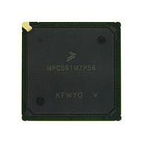
MPC561MZP56 Freescale, MPC561MZP56 Datasheet - Page 1243

MPC561MZP56
Manufacturer Part Number
MPC561MZP56
Description
Manufacturer
Freescale
Datasheet
1.MPC561MZP56.pdf
(1420 pages)
Specifications of MPC561MZP56
Cpu Family
MPC56x
Device Core
PowerPC
Device Core Size
32b
Frequency (max)
56MHz
Interface Type
QSPI/SCI/SPI/UART
Total Internal Ram Size
32KB
# I/os (max)
56
Number Of Timers - General Purpose
22
Operating Supply Voltage (typ)
2.6/5V
Operating Supply Voltage (max)
2.7/5.25V
Operating Supply Voltage (min)
2.5/4.75V
On-chip Adc
2(32-chx10-bit)
Instruction Set Architecture
RISC
Operating Temp Range
-40C to 125C
Operating Temperature Classification
Automotive
Mounting
Surface Mount
Pin Count
388
Package Type
BGA
Program Memory Type
ROMLess
Program Memory Size
Not Required
Lead Free Status / RoHS Status
Not Compliant
Available stocks
Company
Part Number
Manufacturer
Quantity
Price
Company:
Part Number:
MPC561MZP56
Manufacturer:
Freescale Semiconductor
Quantity:
10 000
Company:
Part Number:
MPC561MZP56R2
Manufacturer:
Freescale Semiconductor
Quantity:
10 000
- Current page: 1243 of 1420
- Download datasheet (11Mb)
Note: (V
Freescale Semiconductor
CLKOUT
DD
= 2.6 V ± 0.1 V, V
1
2
3
4
5
29
30
56-MHz operation is available as an option. Some parts (without the 56-MHz option) will operate at a
maximum frequency of 40 MHz.
The timing for BR output is relevant when the MPC561/MPC563 is
selected to work with external bus arbiter. The timing for BG output is relevant when the
MPC561/MPC563 is selected to work with internal bus arbiter.
The setup times required for TA, TEA, and BI are relevant only when they are supplied by the external
device (and not the memory controller).
The maximum value of spec 8 for DATA[0:31] pins must be extended by 1.1 ns if the pins have been
precharged to greater than V
the max. value of VDATAPC. This is currently specified at 3.1 V. The 1.1 ns addition to spec 8 reflects
the expected timing degradation for 3.1 V.
The timing 27 refers to CS when ACS = ‘00’ and to WE[0:3]/BE[0:3] when CSNT = ‘0’.
The D[0:31] input timings 17 and 18 refer to the rising edge of the CLKOUT
in which the TA input signal is asserted.
TS valid to CLKOUT Rising
Edge (Setup Time)
CLKOUT Rising Edge to TS
Valid (Hold Time).
Characteristic
DDH
= 5.0 V ± 0.25 V, T
Table F-10. Bus Operation Timing (continued)
MPC561/MPC563 Reference Manual, Rev. 1.2
5
4
DDL
Figure F-10. CLKOUT Pin Timing
. This is the case if an external slave device on the bus is running at
A
= T
Min
L
7
5
NOTE
to T
40 MHz
H
, 50 pF load unless noted otherwise)
Max
3
Min
1
5
5
56 MHz
2
1
Max
Electrical Characteristics
Unit
ns
ns
F-27
Related parts for MPC561MZP56
Image
Part Number
Description
Manufacturer
Datasheet
Request
R

Part Number:
Description:
MPC5 1K0 5%
Manufacturer:
TE Connectivity
Datasheet:

Part Number:
Description:
MPC5 500R 5%
Manufacturer:
TE Connectivity
Datasheet:

Part Number:
Description:
MPC5 5K0 5%
Manufacturer:
Tyco Electronics
Datasheet:

Part Number:
Description:
MPC5 5R0 5%
Manufacturer:
Tyco Electronics
Datasheet:

Part Number:
Description:
MPC5 50K 5%
Manufacturer:
Tyco Electronics
Datasheet:

Part Number:
Description:
MPC5 1R0 5%
Manufacturer:
Tyco Electronics
Datasheet:

Part Number:
Description:
TOWER ELEVATOR BOARDS HARDWARE
Manufacturer:
Freescale Semiconductor
Datasheet:

Part Number:
Description:
TOWER SERIAL I/O HARDWARE
Manufacturer:
Freescale Semiconductor
Datasheet:

Part Number:
Description:
LCD MODULE FOR TWR SYSTEM
Manufacturer:
Freescale Semiconductor
Datasheet:

Part Number:
Description:
DAUGHTER LCD WVGA I.MX51
Manufacturer:
Freescale Semiconductor
Datasheet:

Part Number:
Description:
TOWER SYSTEM BOARD MPC5125
Manufacturer:
Freescale Semiconductor
Datasheet:


