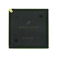
MPC561MZP56 Freescale, MPC561MZP56 Datasheet - Page 727

MPC561MZP56
Manufacturer Part Number
MPC561MZP56
Description
Manufacturer
Freescale
Datasheet
1.MPC561MZP56.pdf
(1420 pages)
Specifications of MPC561MZP56
Cpu Family
MPC56x
Device Core
PowerPC
Device Core Size
32b
Frequency (max)
56MHz
Interface Type
QSPI/SCI/SPI/UART
Total Internal Ram Size
32KB
# I/os (max)
56
Number Of Timers - General Purpose
22
Operating Supply Voltage (typ)
2.6/5V
Operating Supply Voltage (max)
2.7/5.25V
Operating Supply Voltage (min)
2.5/4.75V
On-chip Adc
2(32-chx10-bit)
Instruction Set Architecture
RISC
Operating Temp Range
-40C to 125C
Operating Temperature Classification
Automotive
Mounting
Surface Mount
Pin Count
388
Package Type
BGA
Program Memory Type
ROMLess
Program Memory Size
Not Required
Lead Free Status / RoHS Status
Not Compliant
Available stocks
Company
Part Number
Manufacturer
Quantity
Price
Company:
Part Number:
MPC561MZP56
Manufacturer:
Freescale Semiconductor
Quantity:
10 000
Company:
Part Number:
MPC561MZP56R2
Manufacturer:
Freescale Semiconductor
Quantity:
10 000
- Current page: 727 of 1420
- Download datasheet (11Mb)
16.7.11 Receive Buffer 15 Mask Registers (RX15MSKHI, RX15MSKLO)
The receive buffer 15 mask registers have the same structure as the receive global mask registers and are
used to mask buffer 15.
16.7.12 Error and Status Register (ESTAT)
This register reflects various error conditions, general status, and has the enable bits for three of the
TouCAN interrupt sources. The reported error conditions are those which have occurred since the last time
the register was read. A read clears these bits to zero.
Freescale Semiconductor
SRESET
Bits
0:31
Field
Addr
SRESET
SRESET
Figure 16-18. Receive Buffer 15 Mask Registers: High (RX15MSKHI), Low (RX15MSKLO)
Field MID
Field MID
Addr
MSB
0
ERR
BIT
Name
MIDx
1
MSB
28
14
16
1
1
0
0x30 709A (Rx14MSKLO_A); 0x30 749A (Rx14MSKLO_B); 0x30 789A (Rx14MSKLO_C)
ERR
ACK
0x30 7098 (Rx15MSKHI_A); 0x30 7498 (Rx15MSKHI_B); 0x30 7898 (Rx14MSKHI_C);
2
MID
MID
27
13
17
1
1
1
Table 16-22. RX15MSKHI, RX15MSKLO Field Descriptions
The receive buffer 14 mask registers use 4 bytes.
Base ID mask bits MID[28:18] are used to mask standard or extended format frames.
Extended ID bits MID[17:0] are used to mask only extended format frames.
The RTR/SRR bit of a received frame is never compared to the corresponding bit in the
message buffer ID field. However, remote request frames (RTR = 1) once received, are never
stored into the message buffers. RTR mask bit locations in the mask registers (bits 11 and
31) are always zero, regardless of any write to these bits.
The IDE bit of a received frame is always compared to determine if the message contains a
standard or extended identifier. Its location in the mask registers (bit 12) is always one,
regardless of any write to this bit.
CRC
ERR
3
MID
MID
0x30 70A0 (ESTAT_A); 0x30 74A0 (ESTAT_B); 0x30 78A0 (ESTAT_C)
26
12
18
1
1
Figure 16-19. Error and Status Register (ESTAT)
2
FORM
ERR
MPC561/MPC563 Reference Manual, Rev. 1.2
MID
MID
25
11
4
19
1
1
3
STUFF
MID
MID
24
10
20
ERR
1
1
4
5
MID
MID
23
21
1
9
1
5
WARN
TX
0000_0000_0000_0000
6
MID
MID
22
22
1
8
1
6
WARN
RX
MID
MID
7
21
23
1
7
1
7
Description
IDLE TX/RX
MID
MID
20
24
1
6
1
8
8
MID
MID
19
25
9
1
5
1
9
MID
MID
18
10
26
1
4
1
10
FCS
MID
11
11
27
0
0
3
1
MID
—
12
12
28
1
1
2
1
CAN 2.0B Controller Module
MID
MID
BOFF
17
13
29
INT
1
1
1
13
MID
MID
16
14
30
1
0
1
ERR
INT
14
MID
LSB
15
15
31
1
0
0
WAKE
INT
LSB
15
16-33
Related parts for MPC561MZP56
Image
Part Number
Description
Manufacturer
Datasheet
Request
R

Part Number:
Description:
MPC5 1K0 5%
Manufacturer:
TE Connectivity
Datasheet:

Part Number:
Description:
MPC5 500R 5%
Manufacturer:
TE Connectivity
Datasheet:

Part Number:
Description:
MPC5 5K0 5%
Manufacturer:
Tyco Electronics
Datasheet:

Part Number:
Description:
MPC5 5R0 5%
Manufacturer:
Tyco Electronics
Datasheet:

Part Number:
Description:
MPC5 50K 5%
Manufacturer:
Tyco Electronics
Datasheet:

Part Number:
Description:
MPC5 1R0 5%
Manufacturer:
Tyco Electronics
Datasheet:

Part Number:
Description:
TOWER ELEVATOR BOARDS HARDWARE
Manufacturer:
Freescale Semiconductor
Datasheet:

Part Number:
Description:
TOWER SERIAL I/O HARDWARE
Manufacturer:
Freescale Semiconductor
Datasheet:

Part Number:
Description:
LCD MODULE FOR TWR SYSTEM
Manufacturer:
Freescale Semiconductor
Datasheet:

Part Number:
Description:
DAUGHTER LCD WVGA I.MX51
Manufacturer:
Freescale Semiconductor
Datasheet:

Part Number:
Description:
TOWER SYSTEM BOARD MPC5125
Manufacturer:
Freescale Semiconductor
Datasheet:


