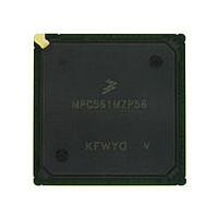
MPC561MZP56 Freescale, MPC561MZP56 Datasheet - Page 182

MPC561MZP56
Manufacturer Part Number
MPC561MZP56
Description
Manufacturer
Freescale
Datasheet
1.MPC561MZP56.pdf
(1420 pages)
Specifications of MPC561MZP56
Cpu Family
MPC56x
Device Core
PowerPC
Device Core Size
32b
Frequency (max)
56MHz
Interface Type
QSPI/SCI/SPI/UART
Total Internal Ram Size
32KB
# I/os (max)
56
Number Of Timers - General Purpose
22
Operating Supply Voltage (typ)
2.6/5V
Operating Supply Voltage (max)
2.7/5.25V
Operating Supply Voltage (min)
2.5/4.75V
On-chip Adc
2(32-chx10-bit)
Instruction Set Architecture
RISC
Operating Temp Range
-40C to 125C
Operating Temperature Classification
Automotive
Mounting
Surface Mount
Pin Count
388
Package Type
BGA
Program Memory Type
ROMLess
Program Memory Size
Not Required
Lead Free Status / RoHS Status
Not Compliant
Available stocks
Company
Part Number
Manufacturer
Quantity
Price
Company:
Part Number:
MPC561MZP56
Manufacturer:
Freescale Semiconductor
Quantity:
10 000
Company:
Part Number:
MPC561MZP56R2
Manufacturer:
Freescale Semiconductor
Quantity:
10 000
- Current page: 182 of 1420
- Download datasheet (11Mb)
Central Processing Unit
The instruction pipeline in the MPC561/MPC563 has four stages:
The history buffer maintains the correct architectural machine state. An exception is taken only when the
instruction is ready to be retired from the machine (i.e., after all previously-issued instructions have
already been retired from the machine). When an exception is taken, all instructions following the
excepting instruction are canceled, (i.e., the values of the affected destination registers are restored using
the values saved in the history buffer during the dispatch stage).
Figure 3-19
Table 3-20
from the time an instruction begins execution until it produces a result that is available for use by a
3-38
1. The dispatch stage is implemented using a distributed mechanism. The central dispatch unit
2. In the execute stage, each execution unit that has an executable instruction executes the instruction.
3. In the writeback stage, the execution unit writes the result to the destination register and reports to
4. In the retirement stage, the history buffer retires instructions in architectural order. An instruction
FETCH
DECODE
READ AND EXECUTE
WRITE BACK (TO DEST REG)
L ADDRESS DRIVE
L DATA
LOAD WRITE BACK
BRANCH DECODE
BRANCH EXECUTE
broadcasts the instruction to all units. In addition, scoreboard information (regarding data
dependencies) is broadcast to each execution unit. Each execution unit decodes the instruction. If
the instruction is not implemented, a program exception is taken. If the instruction is legal and no
data dependency is found, the instruction is accepted by the appropriate execution unit, and the data
found in the destination register is copied to the history buffer. If a data dependency exists, the
machine is stalled until the dependency is resolved.
(For some instructions, this occurs over multiple cycles.)
the history buffer that the instruction is completed.
retires from the machine if it completes execution with no exceptions and if all instructions
preceding it in the instruction stream have finished execution with no exceptions. As many as six
instructions can be retired in one clock.
indicates the latency and blockage for each type of instruction. Latency refers to the interval
shows basic instruction pipeline timing.
MPC561/MPC563 Reference Manual, Rev. 1.2
i1
Figure 3-19. Basic Instruction Pipeline
i1
i1
i1
i2
i1
i1
i2
i1
store
i3
i2
load
i1
i2
Freescale Semiconductor
Related parts for MPC561MZP56
Image
Part Number
Description
Manufacturer
Datasheet
Request
R

Part Number:
Description:
MPC5 1K0 5%
Manufacturer:
TE Connectivity
Datasheet:

Part Number:
Description:
MPC5 500R 5%
Manufacturer:
TE Connectivity
Datasheet:

Part Number:
Description:
MPC5 5K0 5%
Manufacturer:
Tyco Electronics
Datasheet:

Part Number:
Description:
MPC5 5R0 5%
Manufacturer:
Tyco Electronics
Datasheet:

Part Number:
Description:
MPC5 50K 5%
Manufacturer:
Tyco Electronics
Datasheet:

Part Number:
Description:
MPC5 1R0 5%
Manufacturer:
Tyco Electronics
Datasheet:

Part Number:
Description:
TOWER ELEVATOR BOARDS HARDWARE
Manufacturer:
Freescale Semiconductor
Datasheet:

Part Number:
Description:
TOWER SERIAL I/O HARDWARE
Manufacturer:
Freescale Semiconductor
Datasheet:

Part Number:
Description:
LCD MODULE FOR TWR SYSTEM
Manufacturer:
Freescale Semiconductor
Datasheet:

Part Number:
Description:
DAUGHTER LCD WVGA I.MX51
Manufacturer:
Freescale Semiconductor
Datasheet:

Part Number:
Description:
TOWER SYSTEM BOARD MPC5125
Manufacturer:
Freescale Semiconductor
Datasheet:


