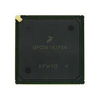
MPC561MZP56 Freescale, MPC561MZP56 Datasheet - Page 916

MPC561MZP56
Manufacturer Part Number
MPC561MZP56
Description
Manufacturer
Freescale
Datasheet
1.MPC561MZP56.pdf
(1420 pages)
Specifications of MPC561MZP56
Cpu Family
MPC56x
Device Core
PowerPC
Device Core Size
32b
Frequency (max)
56MHz
Interface Type
QSPI/SCI/SPI/UART
Total Internal Ram Size
32KB
# I/os (max)
56
Number Of Timers - General Purpose
22
Operating Supply Voltage (typ)
2.6/5V
Operating Supply Voltage (max)
2.7/5.25V
Operating Supply Voltage (min)
2.5/4.75V
On-chip Adc
2(32-chx10-bit)
Instruction Set Architecture
RISC
Operating Temp Range
-40C to 125C
Operating Temperature Classification
Automotive
Mounting
Surface Mount
Pin Count
388
Package Type
BGA
Program Memory Type
ROMLess
Program Memory Size
Not Required
Lead Free Status / RoHS Status
Not Compliant
Available stocks
Company
Part Number
Manufacturer
Quantity
Price
Company:
Part Number:
MPC561MZP56
Manufacturer:
Freescale Semiconductor
Quantity:
10 000
Company:
Part Number:
MPC561MZP56R2
Manufacturer:
Freescale Semiconductor
Quantity:
10 000
- Current page: 916 of 1420
- Download datasheet (11Mb)
Development Support
The following sections define how this information is generated and how it should be used to reconstruct
the program trace. The issue of data compression that could reduce the amount of memory needed by the
debug system is also mentioned.
23.1.1
Program Trace Cycle
To allow visibility of the events happening in the machine a few dedicated pins are used and a special bus
cycle attribute, program trace cycle, is defined.
The program trace cycle attribute is attached to all fetch cycles resulting from indirect flow changes. When
program trace recording is needed, make sure these cycles are visible on the external bus.
The VSYNC indication, when asserted, forces all fetch cycles marked with the program trace cycle
attribute to be visible on the external bus even if their data is found in one of the internal devices. To enable
the external hardware to properly synchronize with the internal activity of the CPU, the assertion and
negation of VSYNC forces the machine to synchronize. The first fetch after this synchronization is marked
as a program trace cycle and is visible on the external bus. For more information on the activity of the
external hardware during program trace refer to
Section 23.1.4, “External
Hardware.”
In order to keep the pin count of the chip as low as possible, VSYNC is not implemented as one of the
chip’s external pins. It is asserted and negated using the serial interface implemented in the development
port. For more information on this interface refer to
Section 23.4, “Development
Port.”
Forcing the CPU to show all fetch cycles marked with the program trace cycle attribute can be done either
by asserting the VSYNC pin (as mentioned above) or by programming the fetch show cycle bits in the
instruction support control register, ICTRL. For more information refer to
Section 23.1.5, “Instruction
Fetch Show Cycle
Control.”
When the VSYNC indication is asserted, all fetch cycles marked with the program trace cycle attribute are
made visible on the external bus. These cycles can generate regular bus cycles (address phase and data
phase) when the instructions reside only in one of the external devices. Or, they can generate address-only
cycles when the instructions reside in one of the internal devices (internal memory, etc.).
When VSYNC is asserted, some performance degradation is expected due to the additional external bus
cycles. However, since this performance degradation is expected to be very small, it is possible to program
the machine to show all indirect flow changes. In this way, the machine will always perform the additional
external bus cycles and maintain exactly the same behavior both when VSYNC is asserted and when it is
negated. For more information refer to
Section 23.6.10, “L-Bus Support Control Register
2.”
The status pins are divided into two groups and one special case listed in the following sections.
23.1.1.1
Instruction Queue Status Pins — VF [0:2]
Instruction queue status pins denote the type of the last fetched instruction or how many instructions were
flushed from the instruction queue. These status pins are used for both functions because queue flushes
only happen in clocks that there is no fetch type information to be reported.
Possible instruction types are defined in
Table
23-1.
MPC561/MPC563 Reference Manual, Rev. 1.2
23-2
Freescale Semiconductor
Related parts for MPC561MZP56
Image
Part Number
Description
Manufacturer
Datasheet
Request
R

Part Number:
Description:
MPC5 1K0 5%
Manufacturer:
TE Connectivity
Datasheet:

Part Number:
Description:
MPC5 500R 5%
Manufacturer:
TE Connectivity
Datasheet:

Part Number:
Description:
MPC5 5K0 5%
Manufacturer:
Tyco Electronics
Datasheet:

Part Number:
Description:
MPC5 5R0 5%
Manufacturer:
Tyco Electronics
Datasheet:

Part Number:
Description:
MPC5 50K 5%
Manufacturer:
Tyco Electronics
Datasheet:

Part Number:
Description:
MPC5 1R0 5%
Manufacturer:
Tyco Electronics
Datasheet:

Part Number:
Description:
TOWER ELEVATOR BOARDS HARDWARE
Manufacturer:
Freescale Semiconductor
Datasheet:

Part Number:
Description:
TOWER SERIAL I/O HARDWARE
Manufacturer:
Freescale Semiconductor
Datasheet:

Part Number:
Description:
LCD MODULE FOR TWR SYSTEM
Manufacturer:
Freescale Semiconductor
Datasheet:

Part Number:
Description:
DAUGHTER LCD WVGA I.MX51
Manufacturer:
Freescale Semiconductor
Datasheet:

Part Number:
Description:
TOWER SYSTEM BOARD MPC5125
Manufacturer:
Freescale Semiconductor
Datasheet:


