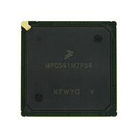
MPC561MZP56 Freescale, MPC561MZP56 Datasheet - Page 118

MPC561MZP56
Manufacturer Part Number
MPC561MZP56
Description
Manufacturer
Freescale
Datasheet
1.MPC561MZP56.pdf
(1420 pages)
Specifications of MPC561MZP56
Cpu Family
MPC56x
Device Core
PowerPC
Device Core Size
32b
Frequency (max)
56MHz
Interface Type
QSPI/SCI/SPI/UART
Total Internal Ram Size
32KB
# I/os (max)
56
Number Of Timers - General Purpose
22
Operating Supply Voltage (typ)
2.6/5V
Operating Supply Voltage (max)
2.7/5.25V
Operating Supply Voltage (min)
2.5/4.75V
On-chip Adc
2(32-chx10-bit)
Instruction Set Architecture
RISC
Operating Temp Range
-40C to 125C
Operating Temperature Classification
Automotive
Mounting
Surface Mount
Pin Count
388
Package Type
BGA
Program Memory Type
ROMLess
Program Memory Size
Not Required
Lead Free Status / RoHS Status
Not Compliant
Available stocks
Company
Part Number
Manufacturer
Quantity
Price
Company:
Part Number:
MPC561MZP56
Manufacturer:
Freescale Semiconductor
Quantity:
10 000
Company:
Part Number:
MPC561MZP56R2
Manufacturer:
Freescale Semiconductor
Quantity:
10 000
- Current page: 118 of 1420
- Download datasheet (11Mb)
Signal Descriptions
2.2.1
Table 2-2
MPC561/MPC563. Most of the signal functions are controlled by the PDMCR2 register.
2-20
1
2
3
4
5
6
VSS
IRAMSTBY
This is the function after PORESET/TRST and HRESET.
This signal also included the MDO5 function on the K27S mask set of the MPC561.
This signal was ECK on K27S mask set of MPC561.
Only the MCP563/MPC564 have Flash memory.
The input only applies in legacy mode.
C_CNTX0 and C_CNRX0 can be shared either with the MIOS14 GPIO pins (MPIO32B12, MPIO32B11) or with the QSMCM
SC12 pins (TXD2 / QGPO2, RXD2 / QGPI2). The selection is made by the TCNC bits in the PDMCR2 register. Refer to
Section 2.4, “Pad Module Configuration Register
Signal Name
describes the signal multiplexing that occurs between different modules of the
MPC561/MPC563 Signal Multiplexing
VFLS0/MPIO32B3/MSEO
TXD2/QGPO2/C_CNTX0
MPIO32B13/PPM_TCLK
RXD2/QGPI2/C_CNRX0
C_CNTX0/MPIO32B12,
C_CNRX0/MPIO32B11
VF0/MPIO32B0/MDO1,
VF1/MPIO32B1/MCKO,
MPIO32B14/PPM_RX0
MPIO32B15/PPM_TX0
VF2/MPIO32B2/MSEI,
MPIO32B8/MPWM20,
MPIO32B9/MPWM21
MPIO32B6/MPWM4,
MPIO32B7/MPWM5,
MPWM3/PPM_RX1
MPWM2/PPM_TX1
MPIO32B5/MDO5
Signal Name
Table 2-1. MPC561/MPC563 Signal Descriptions (continued)
Signals
No. of
1
1
Table 2-2. MPC561/MPC563 Signal Sharing
MPC561/MPC563 Reference Manual, Rev. 1.2
Type
I
I
VSS
IRAMSTBY
Function after
TouCAN shared with MIOS14 GPIO
TouCAN shared with QSMCM SCI2
READI submodule shared with MIOS14 GPIO
MIOS14 PWM submodule shared with MIOS14 GPIO
Debug pins shared with MIOS14 GPIO and READI
PPM submodule shared with MIOS14 GPIO
PPM submodule shared with MIOS14 PWM submodule
(PDMCR2).”
Reset
1
VSS. Zero supply/ground level for internal logic/external
bus.
SRAM Keep-Alive Power. This is an input current source for
an internal regulator that supplies voltage to all SRAM
modules in standby mode. This pad connects through a
voltage regulator and a voltage switch to the following
modules: CALRAM (32-Kbyte SRAM), DPTRAM (8-Kbyte
SRAM), BBC DECRAM (2-Kbyte vocabulary SRAM).
Module Sharing
Description
Freescale Semiconductor
Related parts for MPC561MZP56
Image
Part Number
Description
Manufacturer
Datasheet
Request
R

Part Number:
Description:
MPC5 1K0 5%
Manufacturer:
TE Connectivity
Datasheet:

Part Number:
Description:
MPC5 500R 5%
Manufacturer:
TE Connectivity
Datasheet:

Part Number:
Description:
MPC5 5K0 5%
Manufacturer:
Tyco Electronics
Datasheet:

Part Number:
Description:
MPC5 5R0 5%
Manufacturer:
Tyco Electronics
Datasheet:

Part Number:
Description:
MPC5 50K 5%
Manufacturer:
Tyco Electronics
Datasheet:

Part Number:
Description:
MPC5 1R0 5%
Manufacturer:
Tyco Electronics
Datasheet:

Part Number:
Description:
TOWER ELEVATOR BOARDS HARDWARE
Manufacturer:
Freescale Semiconductor
Datasheet:

Part Number:
Description:
TOWER SERIAL I/O HARDWARE
Manufacturer:
Freescale Semiconductor
Datasheet:

Part Number:
Description:
LCD MODULE FOR TWR SYSTEM
Manufacturer:
Freescale Semiconductor
Datasheet:

Part Number:
Description:
DAUGHTER LCD WVGA I.MX51
Manufacturer:
Freescale Semiconductor
Datasheet:

Part Number:
Description:
TOWER SYSTEM BOARD MPC5125
Manufacturer:
Freescale Semiconductor
Datasheet:


