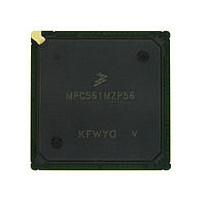
MPC561MZP56 Freescale, MPC561MZP56 Datasheet - Page 642

MPC561MZP56
Manufacturer Part Number
MPC561MZP56
Description
Manufacturer
Freescale
Datasheet
1.MPC561MZP56.pdf
(1420 pages)
Specifications of MPC561MZP56
Cpu Family
MPC56x
Device Core
PowerPC
Device Core Size
32b
Frequency (max)
56MHz
Interface Type
QSPI/SCI/SPI/UART
Total Internal Ram Size
32KB
# I/os (max)
56
Number Of Timers - General Purpose
22
Operating Supply Voltage (typ)
2.6/5V
Operating Supply Voltage (max)
2.7/5.25V
Operating Supply Voltage (min)
2.5/4.75V
On-chip Adc
2(32-chx10-bit)
Instruction Set Architecture
RISC
Operating Temp Range
-40C to 125C
Operating Temperature Classification
Automotive
Mounting
Surface Mount
Pin Count
388
Package Type
BGA
Program Memory Type
ROMLess
Program Memory Size
Not Required
Lead Free Status / RoHS Status
Not Compliant
Available stocks
Company
Part Number
Manufacturer
Quantity
Price
Company:
Part Number:
MPC561MZP56
Manufacturer:
Freescale Semiconductor
Quantity:
10 000
Company:
Part Number:
MPC561MZP56R2
Manufacturer:
Freescale Semiconductor
Quantity:
10 000
- Current page: 642 of 1420
- Download datasheet (11Mb)
Queued Serial Multi-Channel Module
Refer to
15.6.3
Seven pins are associated with the QSPI. When not needed by the QSPI, they can be configured for
general-purpose I/O.
determines whether the pins are designated as input or output. The user must initialize DDRQS for the
QSPI to function correctly.
15-24
Bits
4:7
0
1
2
3
The PCS0 bit represents the dual-function PCS0/SS.
1
PCS[3:0] Peripheral chip selects. Use peripheral chip-select bits to select an external device for serial data transfer. More
CONT
CONT
BITSE
Name
CONT
DSCK
MSB
DT
Section 15.6.5, “Master Mode
—
0
QSPI Pins
Continue
0 Control of chip selects returned to PORTQS after transfer is complete.
1 Peripheral chip selects remain asserted after transfer is complete.
Bits per transfer enable
0 Eight bits
1 Number of bits set in BITS field of SPCR0.
Delay after transfer
0 Delay after transfer is 17 ÷ f
1 SPCR1 DTL[7:0] specifies delay after transfer PCS valid to SCK.
PCS to SCK Delay
0 PCS valid to SCK delay is one-half SCK.
1 SPCR1 DSCKL[6:0] specifies delay from PCS valid to SCK.
than one peripheral chip select may be activated at a time, and more than one peripheral chip can be connected
to each PCS pin, provided proper fanout is observed. PCS0 shares a pin with the slave select (SS) signal, which
initiates slave mode serial transfer. If SS is taken low when the QSPI is in master mode, a mode fault occurs.
BITSE
BITSE
Command Control
—
Table 15-20
1
Figure 15-17. CR[0:F] — Command RAM 0x30 51C0, 0x30 51DF
Table 15-19. Command RAM Bit Descriptions
MPC561/MPC563 Reference Manual, Rev. 1.2
DT
DT
—
2
identifies the QSPI pins and their functions. Register DDRQS
Operation” for more information on the command RAM.
SYS
.
DSCK
DSCK
—
3
Description
PCS3
PCS3
—
4
Peripheral Chip Select
PCS2
PCS2
—
5
PCS1
PCS1
—
6
Freescale Semiconductor
PCS0
PCS0
LSB
—
7
1
1
Related parts for MPC561MZP56
Image
Part Number
Description
Manufacturer
Datasheet
Request
R

Part Number:
Description:
MPC5 1K0 5%
Manufacturer:
TE Connectivity
Datasheet:

Part Number:
Description:
MPC5 500R 5%
Manufacturer:
TE Connectivity
Datasheet:

Part Number:
Description:
MPC5 5K0 5%
Manufacturer:
Tyco Electronics
Datasheet:

Part Number:
Description:
MPC5 5R0 5%
Manufacturer:
Tyco Electronics
Datasheet:

Part Number:
Description:
MPC5 50K 5%
Manufacturer:
Tyco Electronics
Datasheet:

Part Number:
Description:
MPC5 1R0 5%
Manufacturer:
Tyco Electronics
Datasheet:

Part Number:
Description:
TOWER ELEVATOR BOARDS HARDWARE
Manufacturer:
Freescale Semiconductor
Datasheet:

Part Number:
Description:
TOWER SERIAL I/O HARDWARE
Manufacturer:
Freescale Semiconductor
Datasheet:

Part Number:
Description:
LCD MODULE FOR TWR SYSTEM
Manufacturer:
Freescale Semiconductor
Datasheet:

Part Number:
Description:
DAUGHTER LCD WVGA I.MX51
Manufacturer:
Freescale Semiconductor
Datasheet:

Part Number:
Description:
TOWER SYSTEM BOARD MPC5125
Manufacturer:
Freescale Semiconductor
Datasheet:


