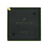
MPC561MZP56 Freescale, MPC561MZP56 Datasheet - Page 259

MPC561MZP56
Manufacturer Part Number
MPC561MZP56
Description
Manufacturer
Freescale
Datasheet
1.MPC561MZP56.pdf
(1420 pages)
Specifications of MPC561MZP56
Cpu Family
MPC56x
Device Core
PowerPC
Device Core Size
32b
Frequency (max)
56MHz
Interface Type
QSPI/SCI/SPI/UART
Total Internal Ram Size
32KB
# I/os (max)
56
Number Of Timers - General Purpose
22
Operating Supply Voltage (typ)
2.6/5V
Operating Supply Voltage (max)
2.7/5.25V
Operating Supply Voltage (min)
2.5/4.75V
On-chip Adc
2(32-chx10-bit)
Instruction Set Architecture
RISC
Operating Temp Range
-40C to 125C
Operating Temperature Classification
Automotive
Mounting
Surface Mount
Pin Count
388
Package Type
BGA
Program Memory Type
ROMLess
Program Memory Size
Not Required
Lead Free Status / RoHS Status
Not Compliant
Available stocks
Company
Part Number
Manufacturer
Quantity
Price
Company:
Part Number:
MPC561MZP56
Manufacturer:
Freescale Semiconductor
Quantity:
10 000
Company:
Part Number:
MPC561MZP56R2
Manufacturer:
Freescale Semiconductor
Quantity:
10 000
- Current page: 259 of 1420
- Download datasheet (11Mb)
Refer to
6.1.7
The time base (TB) is a 64-bit free-running binary counter defined by the MPC500 architecture. The TB
has two independent reference registers which can generate a maskable interrupt when the time base
counter reaches the value programmed in one of the two reference registers. The period of the TB depends
on the driving frequency. The TB is clocked by the TMBCLK clock. The period for the TB is:
The state of TB is not affected by any resets and should be initialized by software. Reads and writes of the
TB are restricted to special instructions. Separate special-purpose registers are defined in the MPC500
architecture for reading and writing the TB. For the MPC561/MPC563 implementation, it is not possible
to read or write the entire TB in a single instruction. Therefore, the mttb and mftb instructions are used to
move the lower half of the time base (TBL) while the mttbu and mftbu instructions are used to move the
upper half (TBU).
Two reference registers are associated with the time base: TBREF0 and TBREF1. A maskable interrupt is
generated when the TB count reaches to the value programmed in one of the two reference registers. Two
status bits in the time base control and status register (TBSCR) indicate which one of the two reference
registers generated the interrupt.
Refer to
Refer to
additional information.
6.1.8
The RTC is a 32-bit counter and pre-divider used to provide a time-of-day indication to the operating
system and application software as show in
Freescale Semiconductor
Section 3.9.5, “Decrementer Register
Section 6.2.2.4, “System Timer
Section 3.9.4, “Time Base Facility (TB) —
Time Base (TB)
Real-Time Clock (RTC)
99
999
9999
999999
9999999
99999999
999999999
(hex) FFFFFFFF
Count Value
Table 6-6. Decrementer Time-Out Periods (continued)
MPC561/MPC563 Reference Manual, Rev. 1.2
Registers,” for diagrams and bit descriptions of TB registers.
Figure
Time-Out @ 4 MHz
T TB
(DEC),” for more information.
10.0 ms
100.0 s
100 µs
1.0 ms
1000 s
4295 s
10.0 s
=
6-7. It is clocked by the PITRTCLK clock. The counter
1.0 s
----------------------------- -
F TMBCLK
OEA,” and to the RCPU Reference Manual for
2
64
Time-Out @ 20 MHz
200 ms
200 µs
200 s
20 µs
859 s
2 ms
2.0 s
20 s
System Configuration and Protection
6-19
Related parts for MPC561MZP56
Image
Part Number
Description
Manufacturer
Datasheet
Request
R

Part Number:
Description:
MPC5 1K0 5%
Manufacturer:
TE Connectivity
Datasheet:

Part Number:
Description:
MPC5 500R 5%
Manufacturer:
TE Connectivity
Datasheet:

Part Number:
Description:
MPC5 5K0 5%
Manufacturer:
Tyco Electronics
Datasheet:

Part Number:
Description:
MPC5 5R0 5%
Manufacturer:
Tyco Electronics
Datasheet:

Part Number:
Description:
MPC5 50K 5%
Manufacturer:
Tyco Electronics
Datasheet:

Part Number:
Description:
MPC5 1R0 5%
Manufacturer:
Tyco Electronics
Datasheet:

Part Number:
Description:
TOWER ELEVATOR BOARDS HARDWARE
Manufacturer:
Freescale Semiconductor
Datasheet:

Part Number:
Description:
TOWER SERIAL I/O HARDWARE
Manufacturer:
Freescale Semiconductor
Datasheet:

Part Number:
Description:
LCD MODULE FOR TWR SYSTEM
Manufacturer:
Freescale Semiconductor
Datasheet:

Part Number:
Description:
DAUGHTER LCD WVGA I.MX51
Manufacturer:
Freescale Semiconductor
Datasheet:

Part Number:
Description:
TOWER SYSTEM BOARD MPC5125
Manufacturer:
Freescale Semiconductor
Datasheet:


