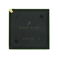
MPC561MZP56 Freescale, MPC561MZP56 Datasheet - Page 858

MPC561MZP56
Manufacturer Part Number
MPC561MZP56
Description
Manufacturer
Freescale
Datasheet
1.MPC561MZP56.pdf
(1420 pages)
Specifications of MPC561MZP56
Cpu Family
MPC56x
Device Core
PowerPC
Device Core Size
32b
Frequency (max)
56MHz
Interface Type
QSPI/SCI/SPI/UART
Total Internal Ram Size
32KB
# I/os (max)
56
Number Of Timers - General Purpose
22
Operating Supply Voltage (typ)
2.6/5V
Operating Supply Voltage (max)
2.7/5.25V
Operating Supply Voltage (min)
2.5/4.75V
On-chip Adc
2(32-chx10-bit)
Instruction Set Architecture
RISC
Operating Temp Range
-40C to 125C
Operating Temperature Classification
Automotive
Mounting
Surface Mount
Pin Count
388
Package Type
BGA
Program Memory Type
ROMLess
Program Memory Size
Not Required
Lead Free Status / RoHS Status
Not Compliant
Available stocks
Company
Part Number
Manufacturer
Quantity
Price
Company:
Part Number:
MPC561MZP56
Manufacturer:
Freescale Semiconductor
Quantity:
10 000
Company:
Part Number:
MPC561MZP56R2
Manufacturer:
Freescale Semiconductor
Quantity:
10 000
- Current page: 858 of 1420
- Download datasheet (11Mb)
Dual-Port TPU3 RAM (DPTRAM)
20.3.2
DPTTCR (test register, address 0x30 0002) is used only during factory testing of the MPC561/MPC563,
and, if written, will generate a bus error.
20.3.3
The RAMBAR register is used to specify the 16 MSBs of the starting DPTRAM array location in the
memory map. In order to be accessible in the MPC561/MPC563 memory map, this register must be
programed to 0xFFA0.
This register can be written only once after a reset. This prevents runaway software from inadvertently
re-mapping the array. Since the locking mechanism is triggered by the first write after reset, the base
20-4
Bits
8:15
1:4
0
5
6
7
DPTRAM Test Register (DPTTCR)
RAM Base Address Register (RAMBAR)
MISEN
Name
STOP
RASP
MISF
—
—
Low power stop (sleep) mode
0 DPTRAM clocks running
1 DPTRAM clocks shut down
Only the STOP bit in the DPTMCR may be accessed while the STOP bit is asserted. Accesses
to other DPTRAM registers may result in unpredictable behavior. Note also that the STOP bit
should be set and cleared independently of the other control bits in this register to guarantee
proper operation. Changing the state of other bits while changing the state of the STOP bit may
result in unpredictable behavior.
Refer to
Reserved
Multiple input signature flag. MISF is readable at any time. This flag bit should be polled by the
host to determine if the MISC has completed reading the DPTRAM. If MISF is set, the host
should read the MISRH and MISRL registers to obtain the DPTRAM signature.
0 First signature not ready
1 MISC has read entire DPTRAM. Signature is latched in MISRH and MISRL and is ready to
Multiple input signature enable. MISEN is readable and writable at any time. The MISC will only
operate when this bit is set and the MPC561/MPC563 is in TPU3 emulation mode. When
enabled, the MISC will continuously cycle through the DPTRAM addresses, reading each and
adding the contents to the MISR. In order to save power, the MISC can be disabled by clearing
the MISEN bit.
0 MISC disabled
1 MISC enabled
RAM area supervisor/user program/data. The DPTRAM array may be placed in supervisor or
unrestricted Space. When placed in supervisor space, (RASP = 1), only a supervisor may
access the array. If a supervisor program is accessing the array, normal read/write operation will
occur. If a user program is attempting to access the array, the access will be ignored and the
address may be decoded externally.
0 Both supervisor and user access to DPTRAM allowed
1 Supervisor access only to DPTRAM allowed
Reserved. These bits are used for the IARB (interrupt arbitration ID) field in TPU3
implementations that use hardware interrupt arbitration.
be read.
Section 20.4.4, “Stop
MPC561/MPC563 Reference Manual, Rev. 1.2
Table 20-2. DPTMCR Bit Settings
Operation” for more information.
Description
Freescale Semiconductor
Related parts for MPC561MZP56
Image
Part Number
Description
Manufacturer
Datasheet
Request
R

Part Number:
Description:
MPC5 1K0 5%
Manufacturer:
TE Connectivity
Datasheet:

Part Number:
Description:
MPC5 500R 5%
Manufacturer:
TE Connectivity
Datasheet:

Part Number:
Description:
MPC5 5K0 5%
Manufacturer:
Tyco Electronics
Datasheet:

Part Number:
Description:
MPC5 5R0 5%
Manufacturer:
Tyco Electronics
Datasheet:

Part Number:
Description:
MPC5 50K 5%
Manufacturer:
Tyco Electronics
Datasheet:

Part Number:
Description:
MPC5 1R0 5%
Manufacturer:
Tyco Electronics
Datasheet:

Part Number:
Description:
TOWER ELEVATOR BOARDS HARDWARE
Manufacturer:
Freescale Semiconductor
Datasheet:

Part Number:
Description:
TOWER SERIAL I/O HARDWARE
Manufacturer:
Freescale Semiconductor
Datasheet:

Part Number:
Description:
LCD MODULE FOR TWR SYSTEM
Manufacturer:
Freescale Semiconductor
Datasheet:

Part Number:
Description:
DAUGHTER LCD WVGA I.MX51
Manufacturer:
Freescale Semiconductor
Datasheet:

Part Number:
Description:
TOWER SYSTEM BOARD MPC5125
Manufacturer:
Freescale Semiconductor
Datasheet:


