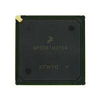
MPC561MZP56 Freescale, MPC561MZP56 Datasheet - Page 605

MPC561MZP56
Manufacturer Part Number
MPC561MZP56
Description
Manufacturer
Freescale
Datasheet
1.MPC561MZP56.pdf
(1420 pages)
Specifications of MPC561MZP56
Cpu Family
MPC56x
Device Core
PowerPC
Device Core Size
32b
Frequency (max)
56MHz
Interface Type
QSPI/SCI/SPI/UART
Total Internal Ram Size
32KB
# I/os (max)
56
Number Of Timers - General Purpose
22
Operating Supply Voltage (typ)
2.6/5V
Operating Supply Voltage (max)
2.7/5.25V
Operating Supply Voltage (min)
2.5/4.75V
On-chip Adc
2(32-chx10-bit)
Instruction Set Architecture
RISC
Operating Temp Range
-40C to 125C
Operating Temperature Classification
Automotive
Mounting
Surface Mount
Pin Count
388
Package Type
BGA
Program Memory Type
ROMLess
Program Memory Size
Not Required
Lead Free Status / RoHS Status
Not Compliant
Available stocks
Company
Part Number
Manufacturer
Quantity
Price
Company:
Part Number:
MPC561MZP56
Manufacturer:
Freescale Semiconductor
Quantity:
10 000
Company:
Part Number:
MPC561MZP56R2
Manufacturer:
Freescale Semiconductor
Quantity:
10 000
- Current page: 605 of 1420
- Download datasheet (11Mb)
Recall QS = 0 => Queues disabled; QS = 8 => Q1 active, Q2 disabled; QS= 4 => Q1 paused, Q2 disabled.
A time separator was provided between the triggers and end of conversion (EOC). The relationship to
QCLK displayed is not guaranteed.
CWPQ1 or CWPQ2 typically lag CWP and only match CWP when the associated queue is inactive.
Another way to view CWPQ1(2) is that these registers update when EOC triggers the result register to be
written.
When the pause bit is set (CCW0), please note that CWP does not increment until triggered. When the
pause is not set (CCW1), the CWP increments with EOC.
The conversion results Q1 RES(x) show the result associated with CCW(x). So that R0 represents the
result associated with CCW0.
Example 2 below shows the timing for conversions in gated mode single-scan with the
same assumptions as example 1 except:
When the gate closes and opens again the conversions start with the first CCW in Q1.
When the gate closes the active conversion completes before the queue goes idle.
When Q1 completes both the CF1 bit sets and the SSE bit clears.
Freescale Semiconductor
•
•
•
•
QCLK
Trig1
EOC
QS
CWP
CWPQ1
Q1 RES
Q1 RES shows relative result register updates
No pause bits set in any CCW
External trigger gated single-scan mode for Q1
Single-scan bit is set
LAST
0
Figure 14-44. External Trigger Mode (Positive Edge) Timing with Pause
LAST
4
8
MPC561/MPC563 Reference Manual, Rev. 1.2
CCW0
Conversion time is >= 14 QCLKS
Time between triggers
4
R0
CCW0
CCW1
QADC64E Enhanced Mode Operation
8
CCW1
R1
CCW2
14-63
Related parts for MPC561MZP56
Image
Part Number
Description
Manufacturer
Datasheet
Request
R

Part Number:
Description:
MPC5 1K0 5%
Manufacturer:
TE Connectivity
Datasheet:

Part Number:
Description:
MPC5 500R 5%
Manufacturer:
TE Connectivity
Datasheet:

Part Number:
Description:
MPC5 5K0 5%
Manufacturer:
Tyco Electronics
Datasheet:

Part Number:
Description:
MPC5 5R0 5%
Manufacturer:
Tyco Electronics
Datasheet:

Part Number:
Description:
MPC5 50K 5%
Manufacturer:
Tyco Electronics
Datasheet:

Part Number:
Description:
MPC5 1R0 5%
Manufacturer:
Tyco Electronics
Datasheet:

Part Number:
Description:
TOWER ELEVATOR BOARDS HARDWARE
Manufacturer:
Freescale Semiconductor
Datasheet:

Part Number:
Description:
TOWER SERIAL I/O HARDWARE
Manufacturer:
Freescale Semiconductor
Datasheet:

Part Number:
Description:
LCD MODULE FOR TWR SYSTEM
Manufacturer:
Freescale Semiconductor
Datasheet:

Part Number:
Description:
DAUGHTER LCD WVGA I.MX51
Manufacturer:
Freescale Semiconductor
Datasheet:

Part Number:
Description:
TOWER SYSTEM BOARD MPC5125
Manufacturer:
Freescale Semiconductor
Datasheet:


