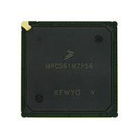
MPC561MZP56 Freescale, MPC561MZP56 Datasheet - Page 941

MPC561MZP56
Manufacturer Part Number
MPC561MZP56
Description
Manufacturer
Freescale
Datasheet
1.MPC561MZP56.pdf
(1420 pages)
Specifications of MPC561MZP56
Cpu Family
MPC56x
Device Core
PowerPC
Device Core Size
32b
Frequency (max)
56MHz
Interface Type
QSPI/SCI/SPI/UART
Total Internal Ram Size
32KB
# I/os (max)
56
Number Of Timers - General Purpose
22
Operating Supply Voltage (typ)
2.6/5V
Operating Supply Voltage (max)
2.7/5.25V
Operating Supply Voltage (min)
2.5/4.75V
On-chip Adc
2(32-chx10-bit)
Instruction Set Architecture
RISC
Operating Temp Range
-40C to 125C
Operating Temperature Classification
Automotive
Mounting
Surface Mount
Pin Count
388
Package Type
BGA
Program Memory Type
ROMLess
Program Memory Size
Not Required
Lead Free Status / RoHS Status
Not Compliant
Available stocks
Company
Part Number
Manufacturer
Quantity
Price
Company:
Part Number:
MPC561MZP56
Manufacturer:
Freescale Semiconductor
Quantity:
10 000
Company:
Part Number:
MPC561MZP56R2
Manufacturer:
Freescale Semiconductor
Quantity:
10 000
- Current page: 941 of 1420
- Download datasheet (11Mb)
0, debug mode is enabled and the check stop enable bit in the debug enable register (DER) is set, the CPU
enters debug mode rather then the check stop state.
The different actions taken by the CPU when a machine check interrupt is detected are shown in the
following table.
23.3.1.4
If entering debug mode was as a result of any load/store type exception, and therefore the DAR (data
address register) and DSISR (data storage interrupt status register) have some significant value, these two
registers must be saved before any other operation is performed. Failing to save these registers may result
in loss of their value in case of another load/store type exception inside the development software.
Since exceptions are treated differently when in debug mode (refer to
Mode”), there is no need to save machine status save/restore zero register (SRR0) and machine status
save/restore one register (SRR1).
23.3.1.5
When running in debug mode all fetch cycles access the development port regardless of the actual address
of the cycle. All load/store cycles access the real memory system according to the cycle’s address. The data
register of the development port is mapped as a special control register therefore it is accessed using mtspr
and mfspr instructions via special load/store cycles (refer to
Register
Exceptions are treated differently when running in debug mode. When already in debug mode, upon
recognition of an exception, the exception cause register (ECR) is updated according to the event that
caused the exception, a special error indication (ecr_or) is asserted for one clock cycle to report to the
development port that an exception occurred and execution continues in debug mode without any change
in SRR0 and SRR1. ECR_OR is asserted before the next fetch occurs to allow the development system to
detect the excepting instruction.
Freescale Semiconductor
1
2
MSR[ME]
Check stop enable bit in the debug enable register (DER)
Machine check interrupt enable bit in the debug enable register (DER)
(DPDR)”).
0
1
0
0
1
1
Saving Machine State upon Entering Debug Mode
Running in Debug Mode
Enable
Debug
Mode
0
0
1
1
1
1
CHSTPE
Table 23-9. Check Stop State and Debug Mode
X
X
X
X
0
1
MPC561/MPC563 Reference Manual, Rev. 1.2
1
MCIE
X
X
X
X
0
1
2
Detecting a Machine Check Interrupt
Enter the check stop state
Branch to the machine check interrupt
Enter the check stop state
Enter Debug Mode
Branch to the machine check interrupt
Enter Debug Mode
Action Performed by the CPU when
Section 23.6.13, “Development Port Data
Section 23.3.1.5, “Running in Debug
Exception Cause
Register (ECR)
0x2000_0000
0x2000_0000
0x1000_0000
0x2000_0000
0x1000_0000
0x1000_0000
Development Support
Value
23-27
Related parts for MPC561MZP56
Image
Part Number
Description
Manufacturer
Datasheet
Request
R

Part Number:
Description:
MPC5 1K0 5%
Manufacturer:
TE Connectivity
Datasheet:

Part Number:
Description:
MPC5 500R 5%
Manufacturer:
TE Connectivity
Datasheet:

Part Number:
Description:
MPC5 5K0 5%
Manufacturer:
Tyco Electronics
Datasheet:

Part Number:
Description:
MPC5 5R0 5%
Manufacturer:
Tyco Electronics
Datasheet:

Part Number:
Description:
MPC5 50K 5%
Manufacturer:
Tyco Electronics
Datasheet:

Part Number:
Description:
MPC5 1R0 5%
Manufacturer:
Tyco Electronics
Datasheet:

Part Number:
Description:
TOWER ELEVATOR BOARDS HARDWARE
Manufacturer:
Freescale Semiconductor
Datasheet:

Part Number:
Description:
TOWER SERIAL I/O HARDWARE
Manufacturer:
Freescale Semiconductor
Datasheet:

Part Number:
Description:
LCD MODULE FOR TWR SYSTEM
Manufacturer:
Freescale Semiconductor
Datasheet:

Part Number:
Description:
DAUGHTER LCD WVGA I.MX51
Manufacturer:
Freescale Semiconductor
Datasheet:

Part Number:
Description:
TOWER SYSTEM BOARD MPC5125
Manufacturer:
Freescale Semiconductor
Datasheet:


