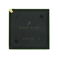
MPC561MZP56 Freescale, MPC561MZP56 Datasheet - Page 164

MPC561MZP56
Manufacturer Part Number
MPC561MZP56
Description
Manufacturer
Freescale
Datasheet
1.MPC561MZP56.pdf
(1420 pages)
Specifications of MPC561MZP56
Cpu Family
MPC56x
Device Core
PowerPC
Device Core Size
32b
Frequency (max)
56MHz
Interface Type
QSPI/SCI/SPI/UART
Total Internal Ram Size
32KB
# I/os (max)
56
Number Of Timers - General Purpose
22
Operating Supply Voltage (typ)
2.6/5V
Operating Supply Voltage (max)
2.7/5.25V
Operating Supply Voltage (min)
2.5/4.75V
On-chip Adc
2(32-chx10-bit)
Instruction Set Architecture
RISC
Operating Temp Range
-40C to 125C
Operating Temperature Classification
Automotive
Mounting
Surface Mount
Pin Count
388
Package Type
BGA
Program Memory Type
ROMLess
Program Memory Size
Not Required
Lead Free Status / RoHS Status
Not Compliant
Available stocks
Company
Part Number
Manufacturer
Quantity
Price
Company:
Part Number:
MPC561MZP56
Manufacturer:
Freescale Semiconductor
Quantity:
10 000
Company:
Part Number:
MPC561MZP56R2
Manufacturer:
Freescale Semiconductor
Quantity:
10 000
- Current page: 164 of 1420
- Download datasheet (11Mb)
Central Processing Unit
3.8
The virtual environment architecture (VEA) defines registers in addition to the UISA register set. The
VEA register set can be accessed by all software with either user- or supervisor-level privileges. Refer to
Section 6.1.7, “Time Base
3.9
The operating environment architecture (OEA) includes a number of SPRs and other registers that are
accessible only by supervisor-level instructions. Some SPRs are RCPU-specific; some RCPU SPRs may
not be implemented in other PowerPC ISA processors, or may not be implemented in the same way.
3.9.1
The machine state register is a 32-bit register that defines the state of the processor. When an exception
occurs, the contents of the MSR are loaded into SRR1, and the MSR is updated to reflect the
exception-processing machine state. The MSR can also be modified by the mtmsr, sc, and rfi instructions.
It can be read by the mfmsr instruction.
Table 3-11
3-20
11
1
2
3
SRESET
SRESET
This bit is available only on code compression-enabled options of the MPC561/MPC563.
Reset Configuration Word
The reset value is defined by the equation "BBCMCR[EN_COMP] AND BBCMCR[EXC_COMP]". At HRESET the
BBCMCR[EN_COMP] and BBCMCR[EXC_COMP] bits recieve their values from RCW bits 21 and 22. The BBCMCR
does not change at SRESET. Thus the DCMPEN reset value may be different on SRESET and HRESET, if software
changes these BBCMCR bits from their reset values.
The reset value is a reset configuration word value extracted from the internal bus line. Refer to
Bits
0:12
13
Field
Field EE
VEA Register Set — Time Base (TB)
OEA Register Set
shows the bit definitions for the MSR.
Machine State Register (MSR)
MSB
16
0
Name
POW
—
000
PR
17
1
Reserved
Power management enable.
0 Power management disabled (normal operation mode)
1 Power management enabled (reduced power mode)
FP
18
2
(TB),” for more information.
(RCW).”
Table 3-11. Machine State Register Bit Descriptions
ME
19
U
3
Figure 3-11. Machine State Register (MSR)
MPC561/MPC563 Reference Manual, Rev. 1.2
FE0
20
4
SE
21
5
0000_0
BE
—
22
6
0000_0000_0000_0000
FE1
23
7
—
24
Description
8
ID1
IP
25
9
2
IR
10
26
000
DR
11
27
—
12
28
DCMPEN
Freescale Semiconductor
POW
Section 7.5.2, “Hard
X
13
29
1
3
RI
14
30
0
00
ILE
LSB
LE
15
31
Related parts for MPC561MZP56
Image
Part Number
Description
Manufacturer
Datasheet
Request
R

Part Number:
Description:
MPC5 1K0 5%
Manufacturer:
TE Connectivity
Datasheet:

Part Number:
Description:
MPC5 500R 5%
Manufacturer:
TE Connectivity
Datasheet:

Part Number:
Description:
MPC5 5K0 5%
Manufacturer:
Tyco Electronics
Datasheet:

Part Number:
Description:
MPC5 5R0 5%
Manufacturer:
Tyco Electronics
Datasheet:

Part Number:
Description:
MPC5 50K 5%
Manufacturer:
Tyco Electronics
Datasheet:

Part Number:
Description:
MPC5 1R0 5%
Manufacturer:
Tyco Electronics
Datasheet:

Part Number:
Description:
TOWER ELEVATOR BOARDS HARDWARE
Manufacturer:
Freescale Semiconductor
Datasheet:

Part Number:
Description:
TOWER SERIAL I/O HARDWARE
Manufacturer:
Freescale Semiconductor
Datasheet:

Part Number:
Description:
LCD MODULE FOR TWR SYSTEM
Manufacturer:
Freescale Semiconductor
Datasheet:

Part Number:
Description:
DAUGHTER LCD WVGA I.MX51
Manufacturer:
Freescale Semiconductor
Datasheet:

Part Number:
Description:
TOWER SYSTEM BOARD MPC5125
Manufacturer:
Freescale Semiconductor
Datasheet:


