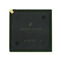
MPC561MZP56 Freescale, MPC561MZP56 Datasheet - Page 357

MPC561MZP56
Manufacturer Part Number
MPC561MZP56
Description
Manufacturer
Freescale
Datasheet
1.MPC561MZP56.pdf
(1420 pages)
Specifications of MPC561MZP56
Cpu Family
MPC56x
Device Core
PowerPC
Device Core Size
32b
Frequency (max)
56MHz
Interface Type
QSPI/SCI/SPI/UART
Total Internal Ram Size
32KB
# I/os (max)
56
Number Of Timers - General Purpose
22
Operating Supply Voltage (typ)
2.6/5V
Operating Supply Voltage (max)
2.7/5.25V
Operating Supply Voltage (min)
2.5/4.75V
On-chip Adc
2(32-chx10-bit)
Instruction Set Architecture
RISC
Operating Temp Range
-40C to 125C
Operating Temperature Classification
Automotive
Mounting
Surface Mount
Pin Count
388
Package Type
BGA
Program Memory Type
ROMLess
Program Memory Size
Not Required
Lead Free Status / RoHS Status
Not Compliant
Available stocks
Company
Part Number
Manufacturer
Quantity
Price
Company:
Part Number:
MPC561MZP56
Manufacturer:
Freescale Semiconductor
Quantity:
10 000
Company:
Part Number:
MPC561MZP56R2
Manufacturer:
Freescale Semiconductor
Quantity:
10 000
- Current page: 357 of 1420
- Download datasheet (11Mb)
Refer to
Controller Option Registers
configuration bits.
9.5.4
The MPC561/MPC563 uses non-wrapping burst transfers to access operands of up to 32 bytes (eight
words). A non-wrapping burst access stops accessing the external device when the word address is modulo
four/eight. Burst configuration is determined by the value of BURST_EN in the SIUMCR register. See
Chapter 5, “Unified System Interface Unit (USIU)
begins the access by supplying a starting address that points to one of the words in the array and requires
the memory to sequentially drive or sample each word on the data bus. The selected slave device must
internally increment ADDR28 and ADDR29 (and ADDR30 in the case of a 16-bit port slave device, and
also ADDR31 in the case of an 8-bit port slave device) of the supplied address for each transfer, causing
the address to reach a four/eight word boundary, and then stop. The address and transfer attributes supplied
by the MPC561/MPC563 remain stable during the transfers. The selected device terminates each transfer
by driving or sampling the word on the data bus and asserting TA.
Freescale Semiconductor
CLKOUT
ADDR[8:31]
TS
RD/WR
TA
OE
Data
Figure 9-11. Read Followed by Write when Pre-Discharge Mode is Enabled, and EHTR is Set
Section 2.4, “Pad Module Configuration Register
Burst Transfer
Read Data
Read Cycle
(OR0–OR3),” for more information on PREDIS_EN, and EHTR
EHTR provides 1 clock
gap to three-state data bus
MPC561/MPC563 Reference Manual, Rev. 1.2
Overview” for further details. The MPC561/MPC563
Pre-discharge
to low voltage
(PDMCR2),” and
Write Cycle
Section 10.9.4, “Memory
Write Data
External Bus Interface
9-17
Related parts for MPC561MZP56
Image
Part Number
Description
Manufacturer
Datasheet
Request
R

Part Number:
Description:
MPC5 1K0 5%
Manufacturer:
TE Connectivity
Datasheet:

Part Number:
Description:
MPC5 500R 5%
Manufacturer:
TE Connectivity
Datasheet:

Part Number:
Description:
MPC5 5K0 5%
Manufacturer:
Tyco Electronics
Datasheet:

Part Number:
Description:
MPC5 5R0 5%
Manufacturer:
Tyco Electronics
Datasheet:

Part Number:
Description:
MPC5 50K 5%
Manufacturer:
Tyco Electronics
Datasheet:

Part Number:
Description:
MPC5 1R0 5%
Manufacturer:
Tyco Electronics
Datasheet:

Part Number:
Description:
TOWER ELEVATOR BOARDS HARDWARE
Manufacturer:
Freescale Semiconductor
Datasheet:

Part Number:
Description:
TOWER SERIAL I/O HARDWARE
Manufacturer:
Freescale Semiconductor
Datasheet:

Part Number:
Description:
LCD MODULE FOR TWR SYSTEM
Manufacturer:
Freescale Semiconductor
Datasheet:

Part Number:
Description:
DAUGHTER LCD WVGA I.MX51
Manufacturer:
Freescale Semiconductor
Datasheet:

Part Number:
Description:
TOWER SYSTEM BOARD MPC5125
Manufacturer:
Freescale Semiconductor
Datasheet:


