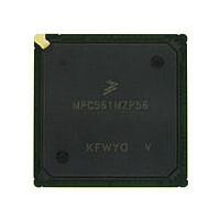
MPC561MZP56 Freescale, MPC561MZP56 Datasheet - Page 882

MPC561MZP56
Manufacturer Part Number
MPC561MZP56
Description
Manufacturer
Freescale
Datasheet
1.MPC561MZP56.pdf
(1420 pages)
Specifications of MPC561MZP56
Cpu Family
MPC56x
Device Core
PowerPC
Device Core Size
32b
Frequency (max)
56MHz
Interface Type
QSPI/SCI/SPI/UART
Total Internal Ram Size
32KB
# I/os (max)
56
Number Of Timers - General Purpose
22
Operating Supply Voltage (typ)
2.6/5V
Operating Supply Voltage (max)
2.7/5.25V
Operating Supply Voltage (min)
2.5/4.75V
On-chip Adc
2(32-chx10-bit)
Instruction Set Architecture
RISC
Operating Temp Range
-40C to 125C
Operating Temperature Classification
Automotive
Mounting
Surface Mount
Pin Count
388
Package Type
BGA
Program Memory Type
ROMLess
Program Memory Size
Not Required
Lead Free Status / RoHS Status
Not Compliant
Available stocks
Company
Part Number
Manufacturer
Quantity
Price
Company:
Part Number:
MPC561MZP56
Manufacturer:
Freescale Semiconductor
Quantity:
10 000
Company:
Part Number:
MPC561MZP56R2
Manufacturer:
Freescale Semiconductor
Quantity:
10 000
- Current page: 882 of 1420
- Download datasheet (11Mb)
CDR3 Flash (UC3F) EEPROM
During power up and power down periods, it is assumed that the reset signal is asserted to prevent
accidental program/erase disturb of the UC3F array.
21.3.2
The UC3F EEPROM control registers are accessible for read or write operation at all times while the
device is powered up and enabled except during reset.
21.3.3
The UC3F EEPROM array is available for a read operation under most conditions while the device is
powered up. Reads of the array are not allowed in the following instances:
The address of an incoming read access is compared to the address for which data is currently held in the
read page buffers. If the data corresponding to the read address is currently held in one of the two read page
buffers, the data is fetched from the appropriate read page buffer. A data fetch from a read page buffer is
an on-page read operation
in one of the read page buffers, 32 bytes of information is fetched from the UC3F array, and the addressed
data is driven onto the data bus. A data fetch from the UC3F array is an off-page read operation.
For information regarding how the two read page buffers in the UC3F EEPROM are associated to array
blocks, refer to
The UC3F module is configured as a page mode memory. The UC3F module uses an internal address
comparator to monitor incoming addresses to determine if the addressed information is stored in a read
page buffer. When the address comparator determines that the requested information is not stored in a read
page buffer, an array off-page read operation retrieves 32 bytes of data from the Flash array and transfers
the addressed data to the data bus.
In the MPC563, the UC3F module contains two 32-byte read page buffers. In the module, one buffer is
dedicated to the most recently accessed instruction fetches and the other read page buffer is dedicated to
the most recently loaded data access.
21-20
•
•
•
•
During reset—When in information or cleared censorship with ACCESS = 0
While the UC3F EEPROM is disabled—See
disabling the UC3F EEPROM
While the UC3F EEPROM is in STOP mode—See
information on STOP mode
While high voltage is applied to the array during program and erase
operation —HVS = 1 or EHV = 1 and not suspended
Register Read and Write Operation
Array Read Operation
After setting/clearing UC3FCTL[HSUS], reset, programming writes, erase
interlock write, setting EHV, clearing SES or setting/clearing SIE, the page
buffers may not contain valid information. The UC3F forces an off-page
read before an on-page read can be accomplished to ensure data coherency.
Section 21.2.2, “UC3F EEPROM Array
Section 21.3.3.1, “Array On-Page Read
MPC561/MPC563 Reference Manual, Rev. 1.2
NOTE
Section 21.3.10,
Addressing.”
Section 21.3.9, “Stop
Operation.” If the data is not contained
“Disabled,” for more information on
Operation,” for more
Freescale Semiconductor
Related parts for MPC561MZP56
Image
Part Number
Description
Manufacturer
Datasheet
Request
R

Part Number:
Description:
MPC5 1K0 5%
Manufacturer:
TE Connectivity
Datasheet:

Part Number:
Description:
MPC5 500R 5%
Manufacturer:
TE Connectivity
Datasheet:

Part Number:
Description:
MPC5 5K0 5%
Manufacturer:
Tyco Electronics
Datasheet:

Part Number:
Description:
MPC5 5R0 5%
Manufacturer:
Tyco Electronics
Datasheet:

Part Number:
Description:
MPC5 50K 5%
Manufacturer:
Tyco Electronics
Datasheet:

Part Number:
Description:
MPC5 1R0 5%
Manufacturer:
Tyco Electronics
Datasheet:

Part Number:
Description:
TOWER ELEVATOR BOARDS HARDWARE
Manufacturer:
Freescale Semiconductor
Datasheet:

Part Number:
Description:
TOWER SERIAL I/O HARDWARE
Manufacturer:
Freescale Semiconductor
Datasheet:

Part Number:
Description:
LCD MODULE FOR TWR SYSTEM
Manufacturer:
Freescale Semiconductor
Datasheet:

Part Number:
Description:
DAUGHTER LCD WVGA I.MX51
Manufacturer:
Freescale Semiconductor
Datasheet:

Part Number:
Description:
TOWER SYSTEM BOARD MPC5125
Manufacturer:
Freescale Semiconductor
Datasheet:


