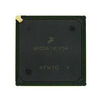
MPC561MZP56 Freescale, MPC561MZP56 Datasheet - Page 850

MPC561MZP56
Manufacturer Part Number
MPC561MZP56
Description
Manufacturer
Freescale
Datasheet
1.MPC561MZP56.pdf
(1420 pages)
Specifications of MPC561MZP56
Cpu Family
MPC56x
Device Core
PowerPC
Device Core Size
32b
Frequency (max)
56MHz
Interface Type
QSPI/SCI/SPI/UART
Total Internal Ram Size
32KB
# I/os (max)
56
Number Of Timers - General Purpose
22
Operating Supply Voltage (typ)
2.6/5V
Operating Supply Voltage (max)
2.7/5.25V
Operating Supply Voltage (min)
2.5/4.75V
On-chip Adc
2(32-chx10-bit)
Instruction Set Architecture
RISC
Operating Temp Range
-40C to 125C
Operating Temperature Classification
Automotive
Mounting
Surface Mount
Pin Count
388
Package Type
BGA
Program Memory Type
ROMLess
Program Memory Size
Not Required
Lead Free Status / RoHS Status
Not Compliant
Available stocks
Company
Part Number
Manufacturer
Quantity
Price
Company:
Part Number:
MPC561MZP56
Manufacturer:
Freescale Semiconductor
Quantity:
10 000
Company:
Part Number:
MPC561MZP56R2
Manufacturer:
Freescale Semiconductor
Quantity:
10 000
- Current page: 850 of 1420
- Download datasheet (11Mb)
Time Processor Unit 3
19-20
11:13
Bits
9:10
14
15
8
Filter Control
000
001
010
011
100
SOFT RST Soft reset. The TPU3 performs an internal reset when both the SOFT RST bit in the TPUMCR2
ETBANK
FPSCK
Name
DTPU
T2CF
Table 19-20. System Clock Frequency/Minimum Guaranteed Detected Pulse
and the STOP bit in TPUMCR are set. The CPU must write zero to the SOFT RST bit to bring
the TPU3 out of reset. The SOFT RST bit must be asserted for at least nine clocks.
0 Normal operation
1 Puts TPU3 in reset until bit is cleared
NOTE: Do not attempt to access any other TPU3 registers when this bit is asserted. When this
bit is asserted, it is the only accessible bit in the register.
Entry table bank select. This field determines the bank where the microcoded entry table is
situated. After reset, this field is 0b00. This control bit field is write once after reset. ETBANK is
used when the microcode contains entry tables not located in the default bank 0. To execute the
ROM functions on this MCU, ETBANK[1:0] must be 00. Refer to
NOTE: This field should not be modified by the programmer unless necessary because of custom
microcode.
Filter prescaler clock. The filter prescaler clock control bit field determines the ratio between
system clock frequency and minimum detectable pulses. The reset value of these bits is zero,
defining the filter clock as four system clocks. Refer to
T2CLK pin filter control. When asserted, the T2CLK input pin is filtered with the same filter clock
that is supplied to the channels. This control bit is write once after reset.
0 Uses fixed four-clock filter
1 T2CLK input pin filtered with same filter clock that is supplied to the channels
Disable TPU3 pins. When the disable TPU3 control pin is asserted, pin TP15 is configured as an
input disable pin. When the TP15 pin value is zero, all TPU3 output pins are three-stated,
regardless of the pins function. The input is not synchronized. This control bit is write once after
reset.
0 TP15 functions as normal TPU3 channel
1 TP15 pin configured as output disable pin. When TP15 pin is low, all TPU3 output pins are in
a high-impedance state, regardless of the pin function.
Divide By
Table 19-18. TPUMCR2 Bit Descriptions (continued)
16
32
64
4
8
MPC561/MPC563 Reference Manual, Rev. 1.2
Table 19-19. Entry Table Bank Location
ETBANK
20 MHz
200 ns
400 ns
800 ns
1.6 µs
3.2 µs
00
01
10
11
Description
Bank
33 MHz
1.94 µs
121 ns
242 ns
485 ns
970 ns
0
1
2
3
Table
19-20.
40 MHz
1.60 µs
100 ns
200 ns
400 ns
800 ns
Table
19-19.
Freescale Semiconductor
56 MHz
1.14 µs
143 ns
286 ns
571 ns
71 ns
Related parts for MPC561MZP56
Image
Part Number
Description
Manufacturer
Datasheet
Request
R

Part Number:
Description:
MPC5 1K0 5%
Manufacturer:
TE Connectivity
Datasheet:

Part Number:
Description:
MPC5 500R 5%
Manufacturer:
TE Connectivity
Datasheet:

Part Number:
Description:
MPC5 5K0 5%
Manufacturer:
Tyco Electronics
Datasheet:

Part Number:
Description:
MPC5 5R0 5%
Manufacturer:
Tyco Electronics
Datasheet:

Part Number:
Description:
MPC5 50K 5%
Manufacturer:
Tyco Electronics
Datasheet:

Part Number:
Description:
MPC5 1R0 5%
Manufacturer:
Tyco Electronics
Datasheet:

Part Number:
Description:
TOWER ELEVATOR BOARDS HARDWARE
Manufacturer:
Freescale Semiconductor
Datasheet:

Part Number:
Description:
TOWER SERIAL I/O HARDWARE
Manufacturer:
Freescale Semiconductor
Datasheet:

Part Number:
Description:
LCD MODULE FOR TWR SYSTEM
Manufacturer:
Freescale Semiconductor
Datasheet:

Part Number:
Description:
DAUGHTER LCD WVGA I.MX51
Manufacturer:
Freescale Semiconductor
Datasheet:

Part Number:
Description:
TOWER SYSTEM BOARD MPC5125
Manufacturer:
Freescale Semiconductor
Datasheet:


