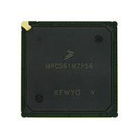
MPC561MZP56 Freescale, MPC561MZP56 Datasheet - Page 129

MPC561MZP56
Manufacturer Part Number
MPC561MZP56
Description
Manufacturer
Freescale
Datasheet
1.MPC561MZP56.pdf
(1420 pages)
Specifications of MPC561MZP56
Cpu Family
MPC56x
Device Core
PowerPC
Device Core Size
32b
Frequency (max)
56MHz
Interface Type
QSPI/SCI/SPI/UART
Total Internal Ram Size
32KB
# I/os (max)
56
Number Of Timers - General Purpose
22
Operating Supply Voltage (typ)
2.6/5V
Operating Supply Voltage (max)
2.7/5.25V
Operating Supply Voltage (min)
2.5/4.75V
On-chip Adc
2(32-chx10-bit)
Instruction Set Architecture
RISC
Operating Temp Range
-40C to 125C
Operating Temperature Classification
Automotive
Mounting
Surface Mount
Pin Count
388
Package Type
BGA
Program Memory Type
ROMLess
Program Memory Size
Not Required
Lead Free Status / RoHS Status
Not Compliant
Available stocks
Company
Part Number
Manufacturer
Quantity
Price
Company:
Part Number:
MPC561MZP56
Manufacturer:
Freescale Semiconductor
Quantity:
10 000
Company:
Part Number:
MPC561MZP56R2
Manufacturer:
Freescale Semiconductor
Quantity:
10 000
- Current page: 129 of 1420
- Download datasheet (11Mb)
Nexus mode is exited by:
2.6
During reset, a 130-µA (maximum) resistor “weakly pulls” all input signals, with the exception of the
power-supply and clock-related signals, to a value based on conditions described in
“Electrical
CLKOUT, HRESET, and SRESET) are pulled only by the pull-up/pull-down.
2.6.1
The reset configuration word (RCW) defines the post-reset functionality of some multiplexed signals. For
details on these signals and how they are configured, refer to Section 7.5.2, “Hard Reset Configuration
Word.”
The 2.6-V bus related signals have selectable output buffer drive strengths that are controlled by the COM0
bit in the USIU’s system clock and reset control register (SCCR). The control is as follows:
2.6.2
While HRESET is asserted, the reset-configuration value is latched from the data bus into various bits on
the part. The function of many signals depends upon the value latched. If the value on the data bus changes,
then the function of various signals may also change. This is especially true if the reset configuration word
(RCW) comes from the Flash, because the Flash does not drive the RCW until 256 clocks after the start of
Freescale Semiconductor
PORESET/TRST
JCOMP/RSTI
•
•
•
•
TMS/EVTI
Drive JCOMP/RSTI high
Hold JCOMP/RSTI low to reset Nexus port
Hold TMS/EVTI high to disable Nexus mode at least 4 clocks before driving JCOMP/RSTI high
Drive JCOMP/RSTI high
Reset State
MDI0
Characteristics.” In reset state, all I/O signals become inputs, and all outputs (except for
0 = 2.6-V bus signals full drive (50-pF load)
1 = 2.6-V bus signals reduced drive (25-pF load)
Signal Functionality Configuration Out of Reset
Signal State During Reset
Figure 2-6. Debug Mode Selection (Nexus)
MPC561/MPC563 Reference Manual, Rev. 1.2
Enable and
Configure Nexus
Nexus On
Nexus Off
Appendix F,
Signal Descriptions
T
2-31
Related parts for MPC561MZP56
Image
Part Number
Description
Manufacturer
Datasheet
Request
R

Part Number:
Description:
MPC5 1K0 5%
Manufacturer:
TE Connectivity
Datasheet:

Part Number:
Description:
MPC5 500R 5%
Manufacturer:
TE Connectivity
Datasheet:

Part Number:
Description:
MPC5 5K0 5%
Manufacturer:
Tyco Electronics
Datasheet:

Part Number:
Description:
MPC5 5R0 5%
Manufacturer:
Tyco Electronics
Datasheet:

Part Number:
Description:
MPC5 50K 5%
Manufacturer:
Tyco Electronics
Datasheet:

Part Number:
Description:
MPC5 1R0 5%
Manufacturer:
Tyco Electronics
Datasheet:

Part Number:
Description:
TOWER ELEVATOR BOARDS HARDWARE
Manufacturer:
Freescale Semiconductor
Datasheet:

Part Number:
Description:
TOWER SERIAL I/O HARDWARE
Manufacturer:
Freescale Semiconductor
Datasheet:

Part Number:
Description:
LCD MODULE FOR TWR SYSTEM
Manufacturer:
Freescale Semiconductor
Datasheet:

Part Number:
Description:
DAUGHTER LCD WVGA I.MX51
Manufacturer:
Freescale Semiconductor
Datasheet:

Part Number:
Description:
TOWER SYSTEM BOARD MPC5125
Manufacturer:
Freescale Semiconductor
Datasheet:


