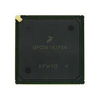
MPC561MZP56 Freescale, MPC561MZP56 Datasheet - Page 348

MPC561MZP56
Manufacturer Part Number
MPC561MZP56
Description
Manufacturer
Freescale
Datasheet
1.MPC561MZP56.pdf
(1420 pages)
Specifications of MPC561MZP56
Cpu Family
MPC56x
Device Core
PowerPC
Device Core Size
32b
Frequency (max)
56MHz
Interface Type
QSPI/SCI/SPI/UART
Total Internal Ram Size
32KB
# I/os (max)
56
Number Of Timers - General Purpose
22
Operating Supply Voltage (typ)
2.6/5V
Operating Supply Voltage (max)
2.7/5.25V
Operating Supply Voltage (min)
2.5/4.75V
On-chip Adc
2(32-chx10-bit)
Instruction Set Architecture
RISC
Operating Temp Range
-40C to 125C
Operating Temperature Classification
Automotive
Mounting
Surface Mount
Pin Count
388
Package Type
BGA
Program Memory Type
ROMLess
Program Memory Size
Not Required
Lead Free Status / RoHS Status
Not Compliant
Available stocks
Company
Part Number
Manufacturer
Quantity
Price
Company:
Part Number:
MPC561MZP56
Manufacturer:
Freescale Semiconductor
Quantity:
10 000
Company:
Part Number:
MPC561MZP56R2
Manufacturer:
Freescale Semiconductor
Quantity:
10 000
- Current page: 348 of 1420
- Download datasheet (11Mb)
External Bus Interface
9.5
This section provides a functional description of the system bus, the signals that control it, and the bus
cycles provided for data transfer operations. It also describes the error conditions, bus arbitration, and reset
operation.
The MPC561/MPC563 generates a system clock output (CLKOUT). This output sets the frequency of
operation for the bus interface directly. Internally, the MPC561/MPC563 uses a phase-lock loop (PLL)
circuit to generate a master clock for all of the MPC561/MPC563 circuitry (including the bus interface)
which is phase-locked to the CLKOUT output signal.
All signals for the MPC561/MPC563 bus interface are specified with respect to the rising edge of the
external CLKOUT and are guaranteed to be sampled as inputs or changed as outputs with respect to that
edge. Since the same clock edge is referenced for driving or sampling the bus signals, the possibility of
clock skew could exist between various modules in a system due to routing or the use of multiple clock
lines. It is the responsibility of the system to handle any such clock skew problems that could occur.
9.5.1
The basic transfer protocol defines the sequence of actions that must occur on the MPC561/MPC563 bus
to perform a complete bus transaction. A simplified scheme of the basic transfer protocol is illustrated in
Figure
The basic transfer protocol provides for an arbitration phase and an address and data transfer phase. The
address phase specifies the address for the transaction and the transfer attributes that describe the
transaction. The data phase performs the transfer of data (if any is to be transferred). The data phase may
transfer a single beat of data (four bytes or less) for nonburst operations, a 4-beat burst of data (4 x 4 bytes),
an 8-beat burst of data (8 x 2 bytes) or a 16-beat burst of data (16 x 1 bytes).
9-8
9-3.
Bus Operations
Signal Name
Basic Transfer Protocol
Arbitration
RETRY
Retry
Table 9-1. MPC561/MPC563 BIU Signals (continued)
Pins
1
MPC561/MPC563 Reference Manual, Rev. 1.2
Address Transfer
Figure 9-3. Basic Transfer Protocol
Active
Low
I/O
O
I
In the case of regular transaction, this signal is driven
by the slave device to indicate that the
MPC561/MPC563 must relinquish the ownership of
the bus and retry the cycle.
When an external master owns the bus and the
internal MPC561/MPC563 bus initiates access to the
external bus at the same time, this signal is used to
cause the external master to relinquish the bus for one
clock to solve the contention.
Data Transfer
Description
Termination
Freescale Semiconductor
Related parts for MPC561MZP56
Image
Part Number
Description
Manufacturer
Datasheet
Request
R

Part Number:
Description:
MPC5 1K0 5%
Manufacturer:
TE Connectivity
Datasheet:

Part Number:
Description:
MPC5 500R 5%
Manufacturer:
TE Connectivity
Datasheet:

Part Number:
Description:
MPC5 5K0 5%
Manufacturer:
Tyco Electronics
Datasheet:

Part Number:
Description:
MPC5 5R0 5%
Manufacturer:
Tyco Electronics
Datasheet:

Part Number:
Description:
MPC5 50K 5%
Manufacturer:
Tyco Electronics
Datasheet:

Part Number:
Description:
MPC5 1R0 5%
Manufacturer:
Tyco Electronics
Datasheet:

Part Number:
Description:
TOWER ELEVATOR BOARDS HARDWARE
Manufacturer:
Freescale Semiconductor
Datasheet:

Part Number:
Description:
TOWER SERIAL I/O HARDWARE
Manufacturer:
Freescale Semiconductor
Datasheet:

Part Number:
Description:
LCD MODULE FOR TWR SYSTEM
Manufacturer:
Freescale Semiconductor
Datasheet:

Part Number:
Description:
DAUGHTER LCD WVGA I.MX51
Manufacturer:
Freescale Semiconductor
Datasheet:

Part Number:
Description:
TOWER SYSTEM BOARD MPC5125
Manufacturer:
Freescale Semiconductor
Datasheet:


