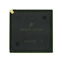
MPC561MZP56 Freescale, MPC561MZP56 Datasheet - Page 737

MPC561MZP56
Manufacturer Part Number
MPC561MZP56
Description
Manufacturer
Freescale
Datasheet
1.MPC561MZP56.pdf
(1420 pages)
Specifications of MPC561MZP56
Cpu Family
MPC56x
Device Core
PowerPC
Device Core Size
32b
Frequency (max)
56MHz
Interface Type
QSPI/SCI/SPI/UART
Total Internal Ram Size
32KB
# I/os (max)
56
Number Of Timers - General Purpose
22
Operating Supply Voltage (typ)
2.6/5V
Operating Supply Voltage (max)
2.7/5.25V
Operating Supply Voltage (min)
2.5/4.75V
On-chip Adc
2(32-chx10-bit)
Instruction Set Architecture
RISC
Operating Temp Range
-40C to 125C
Operating Temperature Classification
Automotive
Mounting
Surface Mount
Pin Count
388
Package Type
BGA
Program Memory Type
ROMLess
Program Memory Size
Not Required
Lead Free Status / RoHS Status
Not Compliant
Available stocks
Company
Part Number
Manufacturer
Quantity
Price
Company:
Part Number:
MPC561MZP56
Manufacturer:
Freescale Semiconductor
Quantity:
10 000
Company:
Part Number:
MPC561MZP56R2
Manufacturer:
Freescale Semiconductor
Quantity:
10 000
- Current page: 737 of 1420
- Download datasheet (11Mb)
Every submodule instantiation is also assigned a number. The number of a given submodule is the block
number of the first block of this submodule.
A submodule is assigned a name made of its acronym followed by its submodule number. For example, if
submodule number 18 were an MPWMSM, it would be named MPWMSM18.
This numbering convention does not apply to the MBISM, the MCPSM, and the MIRSMs. The MBISM
and the MCPSM are unique in the MIOS14 and do not need a number. The MIRSMs are numbered
incrementally starting from zero.
The MIOS14 base address is defined at the chip level and is referred to as the “MIOS14 base address.”
The MIOS14 addressable range is four Kbytes.
The base address of a given implemented submodule within the MIOS14 is the sum of the base address of
the MIOS14 and the submodule number multiplied by eight. Refer to
This does not apply to the MBISM, the MCPSM and the MIRSMs. For these submodules, refer to the
MIOS14 memory map in
17.2.2
In
port signals have a prefix of MPIO. The modulus counter clock and load signals are multiplexed with
MDASM signals.
The MIOS14 input and output signal names are composed of five fields according to the following
convention:
The signal prefix and suffix for the different MIOS14 submodules are as follows:
Freescale Semiconductor
Figure
•
•
•
•
•
•
•
“M”
<submodule short_prefix>
<submodule number>
<signal attribute suffix> (optional)
<bit number> (optional)
MMCSM:
— submodule short_prefix: “MC”
— signal attribute suffix: C for the clock signal
— signal attribute suffix: L for the load signal
— For example, an MMCSM placed as submodule number n would have its corresponding input
MDASM:
— submodule short_prefix: “DA”
— signal attribute suffix: none
17-2, MDASM signals have a prefix MDA, MPWMSM signals have a prefix of MPWM and the
clock pin named MMCnC and its input load pin named MMCnL. MMC6C is input on MDA11
and MMC22C is input on MDA13. The MMC6L is input on MDA12 and MMC22C is input
on MDA14.
Signal Naming Convention
Figure
MPC561/MPC563 Reference Manual, Rev. 1.2
17-2.
Table
Modular Input/Output Subsystem (MIOS14)
17-1.
17-5
Related parts for MPC561MZP56
Image
Part Number
Description
Manufacturer
Datasheet
Request
R

Part Number:
Description:
MPC5 1K0 5%
Manufacturer:
TE Connectivity
Datasheet:

Part Number:
Description:
MPC5 500R 5%
Manufacturer:
TE Connectivity
Datasheet:

Part Number:
Description:
MPC5 5K0 5%
Manufacturer:
Tyco Electronics
Datasheet:

Part Number:
Description:
MPC5 5R0 5%
Manufacturer:
Tyco Electronics
Datasheet:

Part Number:
Description:
MPC5 50K 5%
Manufacturer:
Tyco Electronics
Datasheet:

Part Number:
Description:
MPC5 1R0 5%
Manufacturer:
Tyco Electronics
Datasheet:

Part Number:
Description:
TOWER ELEVATOR BOARDS HARDWARE
Manufacturer:
Freescale Semiconductor
Datasheet:

Part Number:
Description:
TOWER SERIAL I/O HARDWARE
Manufacturer:
Freescale Semiconductor
Datasheet:

Part Number:
Description:
LCD MODULE FOR TWR SYSTEM
Manufacturer:
Freescale Semiconductor
Datasheet:

Part Number:
Description:
DAUGHTER LCD WVGA I.MX51
Manufacturer:
Freescale Semiconductor
Datasheet:

Part Number:
Description:
TOWER SYSTEM BOARD MPC5125
Manufacturer:
Freescale Semiconductor
Datasheet:


