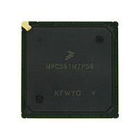
MPC561MZP56 Freescale, MPC561MZP56 Datasheet - Page 786

MPC561MZP56
Manufacturer Part Number
MPC561MZP56
Description
Manufacturer
Freescale
Datasheet
1.MPC561MZP56.pdf
(1420 pages)
Specifications of MPC561MZP56
Cpu Family
MPC56x
Device Core
PowerPC
Device Core Size
32b
Frequency (max)
56MHz
Interface Type
QSPI/SCI/SPI/UART
Total Internal Ram Size
32KB
# I/os (max)
56
Number Of Timers - General Purpose
22
Operating Supply Voltage (typ)
2.6/5V
Operating Supply Voltage (max)
2.7/5.25V
Operating Supply Voltage (min)
2.5/4.75V
On-chip Adc
2(32-chx10-bit)
Instruction Set Architecture
RISC
Operating Temp Range
-40C to 125C
Operating Temperature Classification
Automotive
Mounting
Surface Mount
Pin Count
388
Package Type
BGA
Program Memory Type
ROMLess
Program Memory Size
Not Required
Lead Free Status / RoHS Status
Not Compliant
Available stocks
Company
Part Number
Manufacturer
Quantity
Price
Company:
Part Number:
MPC561MZP56
Manufacturer:
Freescale Semiconductor
Quantity:
10 000
Company:
Part Number:
MPC561MZP56R2
Manufacturer:
Freescale Semiconductor
Quantity:
10 000
- Current page: 786 of 1420
- Download datasheet (11Mb)
Modular Input/Output Subsystem (MIOS14)
The flag bit is a status bit which indicates, when set, that the output period has started and that registers
MPWMPERR and MPWMPULR1 are available for updates when in double-buffered mode. The level of
the resulting interrupt is determined in the MIRSM.
17.10.3.9 MPWMSM Port Functions
The MPWMSM has one dedicated I/O external signal.
The output flip-flop is the basic output of the MPWMSM. Except when the pulse width is at 100% or 0%,
the output flip-flop is reset at the beginning of each period and is set at the beginning of the designated
pulse width until the end of the period. As a software option, the polarity of the signal presented to the
output signal may be the state of the output flip-flop or the inverse of the output flip-flop.
The MPWMSM is connected to an external, input/output signal. When in the disabled mode, the POL bit
(polarity) and the DDR bit (data direction) in the SCR register allow the MPWMSM to be used as an I/O
port.
17.10.3.10 MPWMSM Data Coherency
Byte accesses to MPWMPULR and MPWMPERR are supported, but are not recommended as the transfer
from the primary registers to the secondary registers are done as a 16-bit word transfer.
For most MPWMSM operations, 16-bit accesses are sufficient and long word accesses (32-bit) are treated
as two 16-bit accesses, with one exception — a long word write to the period/pulse width registers. In this
case, if the long word write takes place within the PWM period, there is no visible effect on the output
signal and the new values stored in MPWMPERR and MPWMPULR are ready to be loaded into the buffer
registers at the start of the next period. If, however, the long word write coincides with the end of the
period, then the transfer of values from the primary to the secondary registers is delayed until the end of
the next period; during this period the previous values are used for the period and width. This feature
enables updates of the period and pulse-width values without getting erroneous pulses.
17.10.4 Modular Input/Output Bus (MIOS14) Interface
The MPWMSM is connected to all the signals in the read/write and control bus, to allow data transfer from
and to the MPWMSM registers, and to control the MPWMSM in the different possible situations.
17.10.5 Effect of RESET on MPWMSM
The MPWMSM is affected by reset according to what is described in the section related to register
description.
The MPWMPERR, MPWMPULR, and MPWMCNTR registers, together with the clock prescaler register
bits, must be initialized by software, since they are undefined after hardware reset.
17-54
•
•
The MPWMSM is not using any of the 16-bit counter buses.
The MPWMSM uses the request bus to transmit to the request submodule.
MPC561/MPC563 Reference Manual, Rev. 1.2
Freescale Semiconductor
Related parts for MPC561MZP56
Image
Part Number
Description
Manufacturer
Datasheet
Request
R

Part Number:
Description:
MPC5 1K0 5%
Manufacturer:
TE Connectivity
Datasheet:

Part Number:
Description:
MPC5 500R 5%
Manufacturer:
TE Connectivity
Datasheet:

Part Number:
Description:
MPC5 5K0 5%
Manufacturer:
Tyco Electronics
Datasheet:

Part Number:
Description:
MPC5 5R0 5%
Manufacturer:
Tyco Electronics
Datasheet:

Part Number:
Description:
MPC5 50K 5%
Manufacturer:
Tyco Electronics
Datasheet:

Part Number:
Description:
MPC5 1R0 5%
Manufacturer:
Tyco Electronics
Datasheet:

Part Number:
Description:
TOWER ELEVATOR BOARDS HARDWARE
Manufacturer:
Freescale Semiconductor
Datasheet:

Part Number:
Description:
TOWER SERIAL I/O HARDWARE
Manufacturer:
Freescale Semiconductor
Datasheet:

Part Number:
Description:
LCD MODULE FOR TWR SYSTEM
Manufacturer:
Freescale Semiconductor
Datasheet:

Part Number:
Description:
DAUGHTER LCD WVGA I.MX51
Manufacturer:
Freescale Semiconductor
Datasheet:

Part Number:
Description:
TOWER SYSTEM BOARD MPC5125
Manufacturer:
Freescale Semiconductor
Datasheet:


