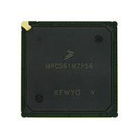
MPC561MZP56 Freescale, MPC561MZP56 Datasheet - Page 666

MPC561MZP56
Manufacturer Part Number
MPC561MZP56
Description
Manufacturer
Freescale
Datasheet
1.MPC561MZP56.pdf
(1420 pages)
Specifications of MPC561MZP56
Cpu Family
MPC56x
Device Core
PowerPC
Device Core Size
32b
Frequency (max)
56MHz
Interface Type
QSPI/SCI/SPI/UART
Total Internal Ram Size
32KB
# I/os (max)
56
Number Of Timers - General Purpose
22
Operating Supply Voltage (typ)
2.6/5V
Operating Supply Voltage (max)
2.7/5.25V
Operating Supply Voltage (min)
2.5/4.75V
On-chip Adc
2(32-chx10-bit)
Instruction Set Architecture
RISC
Operating Temp Range
-40C to 125C
Operating Temperature Classification
Automotive
Mounting
Surface Mount
Pin Count
388
Package Type
BGA
Program Memory Type
ROMLess
Program Memory Size
Not Required
Lead Free Status / RoHS Status
Not Compliant
Available stocks
Company
Part Number
Manufacturer
Quantity
Price
Company:
Part Number:
MPC561MZP56
Manufacturer:
Freescale Semiconductor
Quantity:
10 000
Company:
Part Number:
MPC561MZP56R2
Manufacturer:
Freescale Semiconductor
Quantity:
10 000
- Current page: 666 of 1420
- Download datasheet (11Mb)
Queued Serial Multi-Channel Module
15.7.4
SCxSR contains flags that show SCI operating conditions. These flags are cleared either by SCIx hardware
or by a read/write sequence. The sequence consists of reading the SCxSR (either the upper byte, lower
byte, or the entire half-word) with a flag bit set, then reading (or writing, in the case of flags TDRE and
TC) the SCxDR (either the lower byte or the half-word).
The contents of the two 16-bit registers SCxSR and SCxDR appear as upper and lower half-words,
respectively, when the SCxSR is read into a 32-bit register. An upper byte access of SCxSR is meaningful
only for reads. Note that a word read can simultaneously access both registers SCxSR and SCxDR. This
action clears the receive status flag bits that were set at the time of the read, but does not clear the TDRE
or TC flags. To clear TC, the SCxSR read must be followed by a write to register SCxDR (either the lower
byte or the half-word). The TDRE flag in the status register is read-only.
If an internal SCI signal for setting a status bit comes after the CPU has read the asserted status bits but
before the CPU has read or written the SCxDR, the newly set status bit is not cleared. Instead, SCxSR must
be read again with the bit set and SCxDR must be read or written before the status bit is cleared.
15-48
Bits
10
11
12
13
14
15
SCI Status Register (SCxSR)
Name
RWU
SBK
ILIE
None of the status bits are cleared by reading a status bit while it is set and
then writing zero to that same bit. Instead, the procedure outlined above
must be followed. Note further that reading either byte of SCxSR causes all
16 bits to be accessed, and any status bits already set in either byte are armed
to clear on a subsequent read or write of SCxDR.
RIE
RE
TE
Receiver interrupt enable
0 SCI RDRF and OR interrupts disabled.
1 SCI RDRF and OR interrupts enabled.
Idle-line interrupt enable
0 SCI IDLE interrupts disabled.
1 SCI IDLE interrupts enabled.
Transmitter enable
0 SCI transmitter disabled (TXD pin can be used as general-purpose output)
1 SCI transmitter enabled (TXD pin dedicated to SCI transmitter).
Receiver Enable
0 SCI receiver disabled (RXD pin can be used as general-purpose input).
1 SCI receiver enabled (RXD pin is dedicated to SCI receiver).
Receiver wakeup. Refer to
0 Normal receiver operation (received data recognized).
1 Wakeup mode enabled (received data ignored until receiver is awakened).
Send break
0 Normal operation.
1 Break frame(s) transmitted after completion of current frame.
Table 15-25. SCCxR1 Bit Descriptions (continued)
MPC561/MPC563 Reference Manual, Rev. 1.2
Section 15.7.7.10, “Receiver
NOTE
Description
Wake-Up.”
Freescale Semiconductor
Related parts for MPC561MZP56
Image
Part Number
Description
Manufacturer
Datasheet
Request
R

Part Number:
Description:
MPC5 1K0 5%
Manufacturer:
TE Connectivity
Datasheet:

Part Number:
Description:
MPC5 500R 5%
Manufacturer:
TE Connectivity
Datasheet:

Part Number:
Description:
MPC5 5K0 5%
Manufacturer:
Tyco Electronics
Datasheet:

Part Number:
Description:
MPC5 5R0 5%
Manufacturer:
Tyco Electronics
Datasheet:

Part Number:
Description:
MPC5 50K 5%
Manufacturer:
Tyco Electronics
Datasheet:

Part Number:
Description:
MPC5 1R0 5%
Manufacturer:
Tyco Electronics
Datasheet:

Part Number:
Description:
TOWER ELEVATOR BOARDS HARDWARE
Manufacturer:
Freescale Semiconductor
Datasheet:

Part Number:
Description:
TOWER SERIAL I/O HARDWARE
Manufacturer:
Freescale Semiconductor
Datasheet:

Part Number:
Description:
LCD MODULE FOR TWR SYSTEM
Manufacturer:
Freescale Semiconductor
Datasheet:

Part Number:
Description:
DAUGHTER LCD WVGA I.MX51
Manufacturer:
Freescale Semiconductor
Datasheet:

Part Number:
Description:
TOWER SYSTEM BOARD MPC5125
Manufacturer:
Freescale Semiconductor
Datasheet:


