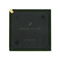
MPC561MZP56 Freescale, MPC561MZP56 Datasheet - Page 316

MPC561MZP56
Manufacturer Part Number
MPC561MZP56
Description
Manufacturer
Freescale
Datasheet
1.MPC561MZP56.pdf
(1420 pages)
Specifications of MPC561MZP56
Cpu Family
MPC56x
Device Core
PowerPC
Device Core Size
32b
Frequency (max)
56MHz
Interface Type
QSPI/SCI/SPI/UART
Total Internal Ram Size
32KB
# I/os (max)
56
Number Of Timers - General Purpose
22
Operating Supply Voltage (typ)
2.6/5V
Operating Supply Voltage (max)
2.7/5.25V
Operating Supply Voltage (min)
2.5/4.75V
On-chip Adc
2(32-chx10-bit)
Instruction Set Architecture
RISC
Operating Temp Range
-40C to 125C
Operating Temperature Classification
Automotive
Mounting
Surface Mount
Pin Count
388
Package Type
BGA
Program Memory Type
ROMLess
Program Memory Size
Not Required
Lead Free Status / RoHS Status
Not Compliant
Available stocks
Company
Part Number
Manufacturer
Quantity
Price
Company:
Part Number:
MPC561MZP56
Manufacturer:
Freescale Semiconductor
Quantity:
10 000
Company:
Part Number:
MPC561MZP56R2
Manufacturer:
Freescale Semiconductor
Quantity:
10 000
- Current page: 316 of 1420
- Download datasheet (11Mb)
Clocks and Power Control
8.5.3
ENGCLK is an output clock with a 50% duty cycle. Its frequency defaults to VCO/128, which is 1/64 of
the main system frequency. ENGCLK frequency can be programmed to the main system frequency
divided by a factor from one to 64, as controlled by the ENGDIV[0:5] bits in the SCCR. ENGCLK can
drive full- or half-strength, or it can also be disabled (remaining in the high state). The drive strength is
controlled by the EECLK[0:1] bits in the SCCR. Disabling ENGCLK can reduce power consumption,
noise, and electromagnetic interference on the printed circuit board.
When the PLL is acquiring lock, the ENGCLK signal is disabled and remains in the low state (provided
that BUCS = 0).
8.6
For limp mode support, clock source switching is supported. If for any reason the clock source for the chip
is not functioning, the option is to switch the system clock to the backup clock ring oscillator, BUCLK.
This circuit consists of a loss-of-clock detector, which sets the LOCS status bit and LOCSS sticky bit in
the PLPRCR. If the LME bit in the SCCR is set, whenever LOCS is asserted, the clock logic switches the
system clock automatically to BUCLK and asserts hard reset to the chip. Switching the system clock to
BUCLK is also possible by software setting the STBUC bit in SCCR. Switching from limp mode to normal
system operation is accomplished by clearing STBUC and LOCSS bits. This operation also asserts hard
reset to the chip.
At HRESET assertion, if the PLL output clock is not valid, the BUCLK will be selected until software
clears LOCSS bit in SCCR. At HRESET assertion, if the PLL output clock is valid, the system will switch
to oscillator/external clock. If during HRESET the PLL loses lock or the clock frequency becomes slower
than the required value, the system will switch to the BUCLK. After HRESET negation the PLL lock
condition does not effect the system clock source selection.
If the LME bit is clear, the switch to the backup clock is disabled and assertion of STBUC bit is ignored.
If the chip is in limp mode, clearing the LME bit switches the system to normal operation and asserts hard
reset to the chip.
Figure 8-8
each state.
8-14
Clock Source Switching
describes the clock switching control logic.
Engineering Clock (ENGCLK)
The full strength ENGCLK setting (SCCR[EECLK]=0b01) selects a 5-V
driver while the half-strength selection (SCCR[EECLK]=0b00) is a 2.6-V
driver.
Skew elimination between CLKOUT and ENGCLK is not guaranteed.
MPC561/MPC563 Reference Manual, Rev. 1.2
NOTE
NOTE
Table 8-3
summarizes the status and control for
Freescale Semiconductor
Related parts for MPC561MZP56
Image
Part Number
Description
Manufacturer
Datasheet
Request
R

Part Number:
Description:
MPC5 1K0 5%
Manufacturer:
TE Connectivity
Datasheet:

Part Number:
Description:
MPC5 500R 5%
Manufacturer:
TE Connectivity
Datasheet:

Part Number:
Description:
MPC5 5K0 5%
Manufacturer:
Tyco Electronics
Datasheet:

Part Number:
Description:
MPC5 5R0 5%
Manufacturer:
Tyco Electronics
Datasheet:

Part Number:
Description:
MPC5 50K 5%
Manufacturer:
Tyco Electronics
Datasheet:

Part Number:
Description:
MPC5 1R0 5%
Manufacturer:
Tyco Electronics
Datasheet:

Part Number:
Description:
TOWER ELEVATOR BOARDS HARDWARE
Manufacturer:
Freescale Semiconductor
Datasheet:

Part Number:
Description:
TOWER SERIAL I/O HARDWARE
Manufacturer:
Freescale Semiconductor
Datasheet:

Part Number:
Description:
LCD MODULE FOR TWR SYSTEM
Manufacturer:
Freescale Semiconductor
Datasheet:

Part Number:
Description:
DAUGHTER LCD WVGA I.MX51
Manufacturer:
Freescale Semiconductor
Datasheet:

Part Number:
Description:
TOWER SYSTEM BOARD MPC5125
Manufacturer:
Freescale Semiconductor
Datasheet:


