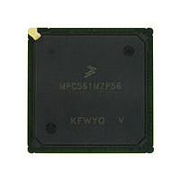
MPC561MZP56 Freescale, MPC561MZP56 Datasheet - Page 1205

MPC561MZP56
Manufacturer Part Number
MPC561MZP56
Description
Manufacturer
Freescale
Datasheet
1.MPC561MZP56.pdf
(1420 pages)
Specifications of MPC561MZP56
Cpu Family
MPC56x
Device Core
PowerPC
Device Core Size
32b
Frequency (max)
56MHz
Interface Type
QSPI/SCI/SPI/UART
Total Internal Ram Size
32KB
# I/os (max)
56
Number Of Timers - General Purpose
22
Operating Supply Voltage (typ)
2.6/5V
Operating Supply Voltage (max)
2.7/5.25V
Operating Supply Voltage (min)
2.5/4.75V
On-chip Adc
2(32-chx10-bit)
Instruction Set Architecture
RISC
Operating Temp Range
-40C to 125C
Operating Temperature Classification
Automotive
Mounting
Surface Mount
Pin Count
388
Package Type
BGA
Program Memory Type
ROMLess
Program Memory Size
Not Required
Lead Free Status / RoHS Status
Not Compliant
Available stocks
Company
Part Number
Manufacturer
Quantity
Price
Company:
Part Number:
MPC561MZP56
Manufacturer:
Freescale Semiconductor
Quantity:
10 000
Company:
Part Number:
MPC561MZP56R2
Manufacturer:
Freescale Semiconductor
Quantity:
10 000
- Current page: 1205 of 1420
- Download datasheet (11Mb)
D.20 Serial Input/Output Port (SIOP)
The serial input/output port (SIOP) TPU3 function uses two or three TPU3 channels to form a uni- or
bidirectional synchronous serial port that can be used to communicate with a wide variety of devices. It
can be used to add serial capabilities to a device without a serial port, or to extend the capabilities of one
with a hardware-synchronous port. The SIOP TPU3 function has been designed to closely resemble the
SIOP hardware port found on some Freescale MCUs.
SIOP operates in master mode (the TPU3 always generates the clock) and has the following programmable
features:
When a transfer of data is complete, the SIOP function notifies the host RCPU by issuing an interrupt
request. The arrangement of the multiple SIOP channels is fixed: the data-out channel is the channel above
the clock channel and the data-in channel is the channel below the clock channel. In clock-only or
uni-directional mode, the unused TPU3 channels are free to run other TPU3 functions. Two possible SIOP
configurations are shown in
D.20.1
Figure D-32
sections describe these parameters.
Freescale Semiconductor
Da ta Out-Chan x+1
Clo c k Out-Chan x
Da ta Out-Cha n x+1
Da ta In-Cha n x-1
Clo c k Out-Chan x
1. Choice of one-channel clock-only, two-channel clock + transmit, two-channel clock + receive, or
2. Freely programmable baud-rate period over a 15-bit range of TCR1 counts
3. Selection of MSB or LSB first shift direction
4. Variable transfer size from 1 to 16 bits
5. Programmable clock polarity
three-channel clock + transmit + receive operating modes
Parameters
shows the host interface areas and parameter RAM for the SIOP function. The following
10-bit output only transfer, LSB first with data valid on clock falling edge
8-bit bidirectional transfer, MSB first with data valid on clock rising edge
Figure D-31
Figure D-31. Two Possible SIOP Configurations
0
7
7
MPC561/MPC563 Reference Manual, Rev. 1.2
6
6
1
2
5
5
4
4
3
3
3
4
2
2
5
1
1
6
0
0
7
8
TPU3 ROM Functions
9
D-53
Related parts for MPC561MZP56
Image
Part Number
Description
Manufacturer
Datasheet
Request
R

Part Number:
Description:
MPC5 1K0 5%
Manufacturer:
TE Connectivity
Datasheet:

Part Number:
Description:
MPC5 500R 5%
Manufacturer:
TE Connectivity
Datasheet:

Part Number:
Description:
MPC5 5K0 5%
Manufacturer:
Tyco Electronics
Datasheet:

Part Number:
Description:
MPC5 5R0 5%
Manufacturer:
Tyco Electronics
Datasheet:

Part Number:
Description:
MPC5 50K 5%
Manufacturer:
Tyco Electronics
Datasheet:

Part Number:
Description:
MPC5 1R0 5%
Manufacturer:
Tyco Electronics
Datasheet:

Part Number:
Description:
TOWER ELEVATOR BOARDS HARDWARE
Manufacturer:
Freescale Semiconductor
Datasheet:

Part Number:
Description:
TOWER SERIAL I/O HARDWARE
Manufacturer:
Freescale Semiconductor
Datasheet:

Part Number:
Description:
LCD MODULE FOR TWR SYSTEM
Manufacturer:
Freescale Semiconductor
Datasheet:

Part Number:
Description:
DAUGHTER LCD WVGA I.MX51
Manufacturer:
Freescale Semiconductor
Datasheet:

Part Number:
Description:
TOWER SYSTEM BOARD MPC5125
Manufacturer:
Freescale Semiconductor
Datasheet:


