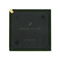
MPC561MZP56 Freescale, MPC561MZP56 Datasheet - Page 107

MPC561MZP56
Manufacturer Part Number
MPC561MZP56
Description
Manufacturer
Freescale
Datasheet
1.MPC561MZP56.pdf
(1420 pages)
Specifications of MPC561MZP56
Cpu Family
MPC56x
Device Core
PowerPC
Device Core Size
32b
Frequency (max)
56MHz
Interface Type
QSPI/SCI/SPI/UART
Total Internal Ram Size
32KB
# I/os (max)
56
Number Of Timers - General Purpose
22
Operating Supply Voltage (typ)
2.6/5V
Operating Supply Voltage (max)
2.7/5.25V
Operating Supply Voltage (min)
2.5/4.75V
On-chip Adc
2(32-chx10-bit)
Instruction Set Architecture
RISC
Operating Temp Range
-40C to 125C
Operating Temperature Classification
Automotive
Mounting
Surface Mount
Pin Count
388
Package Type
BGA
Program Memory Type
ROMLess
Program Memory Size
Not Required
Lead Free Status / RoHS Status
Not Compliant
Available stocks
Company
Part Number
Manufacturer
Quantity
Price
Company:
Part Number:
MPC561MZP56
Manufacturer:
Freescale Semiconductor
Quantity:
10 000
Company:
Part Number:
MPC561MZP56R2
Manufacturer:
Freescale Semiconductor
Quantity:
10 000
- Current page: 107 of 1420
- Download datasheet (11Mb)
Freescale Semiconductor
TMS / EVTI
TDI / DSDI / MDI0
TCK / DSCK / MCKI
TDO / DSDO / MDO0
JCOMP / RSTI
Signal Name
Table 2-1. MPC561/MPC563 Signal Descriptions (continued)
Signals
No. of
1
1
1
1
1
MPC561/MPC563 Reference Manual, Rev. 1.2
Type
O
O
O
I
I
I
I
I
I
I
I
I
I
TMS unless the
Nexus (READI)
port is enabled,
then EVTI.
See
DSDI unless the
Nexus (READI)
port (MDI0) or
JTAG mode
(TDI) is enabled.
See
DSCK unless
the Nexus
(READI) port
(MCKI) or JTAG
mode (TCK) is
enabled.
See
DSDO unless
the Nexus
(READI) port
(MDO0) or JTAG
mode (TDO) is
enabled.
See
See
Function after
Section
Section
Section
Section
Section
Reset
JTAG/BDM/READI
1
2.5.
2.5.
2.5.
2.5.
2.5.
Test Mode Select. This input controls test mode operations
for on-board test logic (JTAG).
EVTI. Event in (EVTI) is level sensitive when configured for
breakpoint generation, otherwise it is edge sensitive.
Test Data In. This input is used for serial test instructions
and test data for on-board test logic (JTAG).
Development Serial Data Input. This input signal is the data
in for the debug port interface. See
“Development
Message Data In. MDI0 is a Nexus input signal used for
downloading configuration information, writes to user
resources, and so forth. Internal latching of MDI occurs on
the rising edge of MCKI.
Test Clock. This input provides a clock for on-board test logic
(JTAG).
Development Serial Clock. This input signal is the clock for
the debug port interface. See
Support,” for details.
Message Clock In. This input line is the input clock to the
READI module for the Nexus message clock input.
Test Data Out. This output is used for serial test instructions
and test data for on-board test logic (JTAG).
Development Serial Data Output. This output signal is the
data-out line of the debug port interface. See
“Development
READI Message Data Out. Message data out: MDO0 is an
output signal used for uploading OTM, BTM, DTM, and
read/write accesses. External latching of MDO occurs on
rising edge of MCKO. Eight MDO signals are implemented.
JTAG Compliancy. This signal enables the IEEE1149.1
JTAG compliant circuitry in the MPC561/MPC563.
0 JTAG disabled
1 JTAG enabled
RSTI. Reset input for the Nexus port.
Support,” for details.
Support,” for details.
Description
Chapter 23, “Development
Chapter 23,
Signal Descriptions
Chapter 23,
2-9
Related parts for MPC561MZP56
Image
Part Number
Description
Manufacturer
Datasheet
Request
R

Part Number:
Description:
MPC5 1K0 5%
Manufacturer:
TE Connectivity
Datasheet:

Part Number:
Description:
MPC5 500R 5%
Manufacturer:
TE Connectivity
Datasheet:

Part Number:
Description:
MPC5 5K0 5%
Manufacturer:
Tyco Electronics
Datasheet:

Part Number:
Description:
MPC5 5R0 5%
Manufacturer:
Tyco Electronics
Datasheet:

Part Number:
Description:
MPC5 50K 5%
Manufacturer:
Tyco Electronics
Datasheet:

Part Number:
Description:
MPC5 1R0 5%
Manufacturer:
Tyco Electronics
Datasheet:

Part Number:
Description:
TOWER ELEVATOR BOARDS HARDWARE
Manufacturer:
Freescale Semiconductor
Datasheet:

Part Number:
Description:
TOWER SERIAL I/O HARDWARE
Manufacturer:
Freescale Semiconductor
Datasheet:

Part Number:
Description:
LCD MODULE FOR TWR SYSTEM
Manufacturer:
Freescale Semiconductor
Datasheet:

Part Number:
Description:
DAUGHTER LCD WVGA I.MX51
Manufacturer:
Freescale Semiconductor
Datasheet:

Part Number:
Description:
TOWER SYSTEM BOARD MPC5125
Manufacturer:
Freescale Semiconductor
Datasheet:


