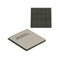
EP4SGX530HH35C2N Altera, EP4SGX530HH35C2N Datasheet - Page 1027

EP4SGX530HH35C2N
Manufacturer Part Number
EP4SGX530HH35C2N
Description
IC STRATIX IV FPGA 530K 1152HBGA
Manufacturer
Altera
Series
Stratix® IV GXr
Datasheets
1.EP4SGX110DF29C3N.pdf
(80 pages)
2.EP4SGX110DF29C3N.pdf
(1154 pages)
3.EP4SGX110DF29C3N.pdf
(432 pages)
4.EP4SGX110DF29C3N.pdf
(22 pages)
5.EP4SGX110DF29C3N.pdf
(30 pages)
6.EP4SGX110DF29C3N.pdf
(72 pages)
7.EP4SGX530HH35C2N.pdf
(1145 pages)
Specifications of EP4SGX530HH35C2N
Number Of Logic Elements/cells
531200
Number Of Labs/clbs
21248
Total Ram Bits
27376
Number Of I /o
564
Voltage - Supply
0.87 V ~ 0.93 V
Mounting Type
Surface Mount
Operating Temperature
0°C ~ 85°C
Package / Case
1152-HBGA
Family Name
Stratix® IV
Number Of Logic Blocks/elements
531200
# Registers
424960
# I/os (max)
560
Process Technology
40nm
Operating Supply Voltage (typ)
900mV
Logic Cells
531200
Ram Bits
28033024
Operating Supply Voltage (min)
0.87V
Operating Supply Voltage (max)
0.93V
Operating Temp Range
0C to 85C
Operating Temperature Classification
Commercial
Mounting
Surface Mount
Pin Count
1152
Package Type
FCHBGA
Lead Free Status / RoHS Status
Lead free / RoHS Compliant
Number Of Gates
-
Lead Free Status / Rohs Status
Compliant
Available stocks
Company
Part Number
Manufacturer
Quantity
Price
- EP4SGX110DF29C3N PDF datasheet
- EP4SGX110DF29C3N PDF datasheet #2
- EP4SGX110DF29C3N PDF datasheet #3
- EP4SGX110DF29C3N PDF datasheet #4
- EP4SGX110DF29C3N PDF datasheet #5
- EP4SGX110DF29C3N PDF datasheet #6
- EP4SGX530HH35C2N PDF datasheet #7
- Current page: 1027 of 1154
- Download datasheet (32Mb)
Chapter 2: Transceiver Design Flow Guide for Stratix IV Devices
Implementation and Integration
February 2011 Altera Corporation
Integrate the Design
1
Gear Boxing Logic
Some protocols require a wider data path than provided by the transceiver interface;
for example, the Interlaken Protocol requires 64/67-bit encoding and decoding, but
the maximum data path interface in the Stratix IV GX transceiver is 40 bits. Therefore,
you must implement gear box logic to interface the 64/67-bit encoder-decoder with
the transceiver interface.
Functional Blocks to Interface with the Transceiver Configured in Basic (PMA Direct) Mode
In Basic (PMA direct) mode, all the PCS functional blocks in the transceiver channel
are disabled. Therefore, you may need to implement the following blocks in the FPGA
fabric:
■
■
■
■
■
After you implement all of the required logic, integrate the transceiver instances with
the remaining logic and provide the appropriate transceiver-FPGA fabric interface
clocking. Synthesize the design using third-party synthesis tools, such as Synopsys
Synplicity or the Quartus II software synthesis tool. This allows you to detect syntax
errors in your design.
If you are using the transceiver in Basic (PMA direct) mode, you must develop all the
PCS functionality in the FPGA fabric.
Word Alignment—To align the byte boundary on the received data.
Byte Deserializer—To increase the data path width to the rest of the user logic and
to reduce the clock frequency of the data path by two.
Phase Compensation FIFO (for bonded channel applications)—In bonded channel
applications in which multiple transceiver channels are connected to the same
upstream system (for example, one Interlaken Protocol link using 24 transceiver
channels). To minimize the global clock routing resources you use, implement a
phase compensation FIFO to interface the receiver side of the transceiver interface
with the logic in the FPGA Fabric.
■
■
With this method, you only use one clock resource and the subsequent
receive-side logic in the FPGA fabric can operate in this single clock domain.
Deskew Logic (for bonded channel applications)—In bonded channel applications
in which multiple transceiver channels are connected to the same upstream
system, the data received between multiple channels are not aligned due to
potential skew in the interconnect and the upstream transmitter system. To
compensate for the skew, use deskew logic in the FPGA fabric.
Encoding/Decoding or Scrambling/Descrambling—Many protocols require the
transmitter data to be encoded or scrambled to maintain signal integrity. This logic
may be required in the FPGA fabric based on your application requirements.
Use the recovered clock from each channel to clock the write side of the phase
compensation FIFO.
Use the recovered clock from any of the channels to clock the read side of the
phase compensation FIFO.
Stratix IV Device Handbook Volume 3
2–9
Related parts for EP4SGX530HH35C2N
Image
Part Number
Description
Manufacturer
Datasheet
Request
R

Part Number:
Description:
CYCLONE II STARTER KIT EP2C20N
Manufacturer:
Altera
Datasheet:

Part Number:
Description:
CPLD, EP610 Family, ECMOS Process, 300 Gates, 16 Macro Cells, 16 Reg., 16 User I/Os, 5V Supply, 35 Speed Grade, 24DIP
Manufacturer:
Altera Corporation
Datasheet:

Part Number:
Description:
CPLD, EP610 Family, ECMOS Process, 300 Gates, 16 Macro Cells, 16 Reg., 16 User I/Os, 5V Supply, 15 Speed Grade, 24DIP
Manufacturer:
Altera Corporation
Datasheet:

Part Number:
Description:
Manufacturer:
Altera Corporation
Datasheet:

Part Number:
Description:
CPLD, EP610 Family, ECMOS Process, 300 Gates, 16 Macro Cells, 16 Reg., 16 User I/Os, 5V Supply, 30 Speed Grade, 24DIP
Manufacturer:
Altera Corporation
Datasheet:

Part Number:
Description:
High-performance, low-power erasable programmable logic devices with 8 macrocells, 10ns
Manufacturer:
Altera Corporation
Datasheet:

Part Number:
Description:
High-performance, low-power erasable programmable logic devices with 8 macrocells, 7ns
Manufacturer:
Altera Corporation
Datasheet:

Part Number:
Description:
Classic EPLD
Manufacturer:
Altera Corporation
Datasheet:

Part Number:
Description:
High-performance, low-power erasable programmable logic devices with 8 macrocells, 10ns
Manufacturer:
Altera Corporation
Datasheet:

Part Number:
Description:
Manufacturer:
Altera Corporation
Datasheet:

Part Number:
Description:
Manufacturer:
Altera Corporation
Datasheet:

Part Number:
Description:
Manufacturer:
Altera Corporation
Datasheet:

Part Number:
Description:
CPLD, EP610 Family, ECMOS Process, 300 Gates, 16 Macro Cells, 16 Reg., 16 User I/Os, 5V Supply, 25 Speed Grade, 24DIP
Manufacturer:
Altera Corporation
Datasheet:


