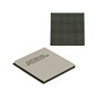
EP4SGX530HH35C2N Altera, EP4SGX530HH35C2N Datasheet - Page 1092

EP4SGX530HH35C2N
Manufacturer Part Number
EP4SGX530HH35C2N
Description
IC STRATIX IV FPGA 530K 1152HBGA
Manufacturer
Altera
Series
Stratix® IV GXr
Datasheets
1.EP4SGX110DF29C3N.pdf
(80 pages)
2.EP4SGX110DF29C3N.pdf
(1154 pages)
3.EP4SGX110DF29C3N.pdf
(432 pages)
4.EP4SGX110DF29C3N.pdf
(22 pages)
5.EP4SGX110DF29C3N.pdf
(30 pages)
6.EP4SGX110DF29C3N.pdf
(72 pages)
7.EP4SGX530HH35C2N.pdf
(1145 pages)
Specifications of EP4SGX530HH35C2N
Number Of Logic Elements/cells
531200
Number Of Labs/clbs
21248
Total Ram Bits
27376
Number Of I /o
564
Voltage - Supply
0.87 V ~ 0.93 V
Mounting Type
Surface Mount
Operating Temperature
0°C ~ 85°C
Package / Case
1152-HBGA
Family Name
Stratix® IV
Number Of Logic Blocks/elements
531200
# Registers
424960
# I/os (max)
560
Process Technology
40nm
Operating Supply Voltage (typ)
900mV
Logic Cells
531200
Ram Bits
28033024
Operating Supply Voltage (min)
0.87V
Operating Supply Voltage (max)
0.93V
Operating Temp Range
0C to 85C
Operating Temperature Classification
Commercial
Mounting
Surface Mount
Pin Count
1152
Package Type
FCHBGA
Lead Free Status / RoHS Status
Lead free / RoHS Compliant
Number Of Gates
-
Lead Free Status / Rohs Status
Compliant
Available stocks
Company
Part Number
Manufacturer
Quantity
Price
- EP4SGX110DF29C3N PDF datasheet
- EP4SGX110DF29C3N PDF datasheet #2
- EP4SGX110DF29C3N PDF datasheet #3
- EP4SGX110DF29C3N PDF datasheet #4
- EP4SGX110DF29C3N PDF datasheet #5
- EP4SGX110DF29C3N PDF datasheet #6
- EP4SGX530HH35C2N PDF datasheet #7
- Current page: 1092 of 1154
- Download datasheet (32Mb)
Chapter 1: DC and Switching Characteristics for Stratix IV Devices
Electrical Characteristics
Table 1–16. Internal Weak Pull-Up Resistor for Stratix IV Devices
Table 1–17. Single-Ended I/O Standards (Part 1 of 2)
April 2011 Altera Corporation
R
Notes to
(1) All I/O pins have an option to enable weak pull-up except configuration, test, and JTAG pins.
(2) Pin pull-up resistance values may be lower if an external source drives the pin higher than V
(3) The internal weak pull-down feature is only available for the JTAG TCK pin. The typical value for this internal weak pull-down resistor is
(4) These specifications are valid with ±10% tolerances to cover changes over PVT.
LVTTL
LVCMOS
Standard
PU
Symbol
I/O
approximately 25 k
Table
1–16:
Value of the I/O pin pull-up resistor before
and during configuration, as well as user
mode if the programmable pull-up resistor
option is enabled.
2.85
2.85
Min
Ω .
V
Schmitt Trigger Input
Stratix IV devices support Schmitt trigger input on the TDI, TMS, TCK, nSTATUS,
nCONFIG, nCE, CONF_DONE, and DCLK pins. A Schmitt trigger feature introduces
hysteresis to the input signal for improved noise immunity, especially for signals with
slow edge rates.
V
Table 1–15. Schmitt Trigger Input Hysteresis Specifications for Stratix IV Devices
Internal Weak Pull-Up Resistor
Table 1–16
I/O Standard Specifications
Table 1–17
(V
standards supported by Stratix IV devices. These tables also show the Stratix IV
device family I/O standard specifications. V
corresponding I
For an explanation of terms used in
on page
CCIO
V
CCIO
Typ
Schmitt
OH
3
3
Symbol
(V)
and V
range for Schmitt trigger inputs in Stratix IV devices.
Description
1–63.
Max
3.15
3.15
lists the weak pull-up resistor values for Stratix IV devices.
through
OL
), and current drive characteristics (I
Hysteresis for Schmitt
trigger input
OH
Table 1–15
Min
-0.3
-0.3
Description
and I
Table 1–22
V
IL
(V)
OL
Max
, respectively.
0.8
0.8
lists the hysteresis specifications across the supported
list the input voltage (V
Stratix IV Device Handbook Volume 4: Device Datasheet and Addendum
Min
1.7
1.7
Table 1–17
V
V
V
V
V
CCIO
CCIO
CCIO
CCIO
CCIO
V
Conditions (V)
Condition (V)
(Note
IH
V
V
V
V
(V)
CCIO
CCIO
CCIO
CCIO
= 3.0 ±5%
= 2.5 ±5%
= 1.8 ±5%
= 1.5 ±5%
= 1.2 ±5%
Max
3.6
3.6
OL
1),
= 3.3
= 2.5
= 1.8
= 1.5
through
and V
(3)
CCIO
OH
(2)
(2)
(2)
(2)
(2)
V
.
Max
OL
and I
OH
0.4
0.2
IH
(V)
Table
values are valid at the
and V
OL
Minimum
) for various I/O
V
1–22, refer to
220
180
110
70
CCIO
V
IL
Value
OH
Min
2.4
), output voltage
- 0.2
(V)
25
25
25
25
25
(4)
I
OL
0.1
(mA) I
“Glossary”
2
Unit
mV
mV
mV
mV
Unit
kΩ
kΩ
kΩ
kΩ
kΩ
OH
-0.1
1–10
-2
(mA)
Related parts for EP4SGX530HH35C2N
Image
Part Number
Description
Manufacturer
Datasheet
Request
R

Part Number:
Description:
CYCLONE II STARTER KIT EP2C20N
Manufacturer:
Altera
Datasheet:

Part Number:
Description:
CPLD, EP610 Family, ECMOS Process, 300 Gates, 16 Macro Cells, 16 Reg., 16 User I/Os, 5V Supply, 35 Speed Grade, 24DIP
Manufacturer:
Altera Corporation
Datasheet:

Part Number:
Description:
CPLD, EP610 Family, ECMOS Process, 300 Gates, 16 Macro Cells, 16 Reg., 16 User I/Os, 5V Supply, 15 Speed Grade, 24DIP
Manufacturer:
Altera Corporation
Datasheet:

Part Number:
Description:
Manufacturer:
Altera Corporation
Datasheet:

Part Number:
Description:
CPLD, EP610 Family, ECMOS Process, 300 Gates, 16 Macro Cells, 16 Reg., 16 User I/Os, 5V Supply, 30 Speed Grade, 24DIP
Manufacturer:
Altera Corporation
Datasheet:

Part Number:
Description:
High-performance, low-power erasable programmable logic devices with 8 macrocells, 10ns
Manufacturer:
Altera Corporation
Datasheet:

Part Number:
Description:
High-performance, low-power erasable programmable logic devices with 8 macrocells, 7ns
Manufacturer:
Altera Corporation
Datasheet:

Part Number:
Description:
Classic EPLD
Manufacturer:
Altera Corporation
Datasheet:

Part Number:
Description:
High-performance, low-power erasable programmable logic devices with 8 macrocells, 10ns
Manufacturer:
Altera Corporation
Datasheet:

Part Number:
Description:
Manufacturer:
Altera Corporation
Datasheet:

Part Number:
Description:
Manufacturer:
Altera Corporation
Datasheet:

Part Number:
Description:
Manufacturer:
Altera Corporation
Datasheet:

Part Number:
Description:
CPLD, EP610 Family, ECMOS Process, 300 Gates, 16 Macro Cells, 16 Reg., 16 User I/Os, 5V Supply, 25 Speed Grade, 24DIP
Manufacturer:
Altera Corporation
Datasheet:


