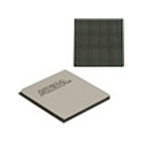
EP4SGX530HH35C2N Altera, EP4SGX530HH35C2N Datasheet - Page 369

EP4SGX530HH35C2N
Manufacturer Part Number
EP4SGX530HH35C2N
Description
IC STRATIX IV FPGA 530K 1152HBGA
Manufacturer
Altera
Series
Stratix® IV GXr
Datasheets
1.EP4SGX110DF29C3N.pdf
(80 pages)
2.EP4SGX110DF29C3N.pdf
(1154 pages)
3.EP4SGX110DF29C3N.pdf
(432 pages)
4.EP4SGX110DF29C3N.pdf
(22 pages)
5.EP4SGX110DF29C3N.pdf
(30 pages)
6.EP4SGX110DF29C3N.pdf
(72 pages)
7.EP4SGX530HH35C2N.pdf
(1145 pages)
Specifications of EP4SGX530HH35C2N
Number Of Logic Elements/cells
531200
Number Of Labs/clbs
21248
Total Ram Bits
27376
Number Of I /o
564
Voltage - Supply
0.87 V ~ 0.93 V
Mounting Type
Surface Mount
Operating Temperature
0°C ~ 85°C
Package / Case
1152-HBGA
Family Name
Stratix® IV
Number Of Logic Blocks/elements
531200
# Registers
424960
# I/os (max)
560
Process Technology
40nm
Operating Supply Voltage (typ)
900mV
Logic Cells
531200
Ram Bits
28033024
Operating Supply Voltage (min)
0.87V
Operating Supply Voltage (max)
0.93V
Operating Temp Range
0C to 85C
Operating Temperature Classification
Commercial
Mounting
Surface Mount
Pin Count
1152
Package Type
FCHBGA
Lead Free Status / RoHS Status
Lead free / RoHS Compliant
Number Of Gates
-
Lead Free Status / Rohs Status
Compliant
Available stocks
Company
Part Number
Manufacturer
Quantity
Price
- EP4SGX110DF29C3N PDF datasheet
- EP4SGX110DF29C3N PDF datasheet #2
- EP4SGX110DF29C3N PDF datasheet #3
- EP4SGX110DF29C3N PDF datasheet #4
- EP4SGX110DF29C3N PDF datasheet #5
- EP4SGX110DF29C3N PDF datasheet #6
- EP4SGX530HH35C2N PDF datasheet #7
- Current page: 369 of 1154
- Download datasheet (32Mb)
Chapter 10: Configuration, Design Security, and Remote System Upgrades in Stratix IV Devices
JTAG Configuration
JTAG Configuration
April 2011 Altera Corporation
f
f
f
1
1
For more information about how to use the USB Blaster, MasterBlaster, ByteBlaster II,
or ByteBlasterMV cables, refer to the following user guides:
■
■
■
■
■
JTAG has developed a specification for boundary-scan testing. This boundary-scan
test (BST) architecture offers the capability to efficiently test components on PCBs
with tight lead spacing. The BST architecture can test pin connections without using
physical test probes and capture functional data while a device is operating normally.
You can also use JTAG circuitry to shift configuration data into the device. The
Quartus II software automatically generates .sofs that you can use for JTAG
configuration with a download cable in the Quartus II software programmer.
For more information about JTAG boundary-scan testing and commands available
using Stratix IV devices, refer to the following documents:
■
■
Stratix IV devices are designed such that JTAG instructions have precedence over any
device configuration modes. Therefore, JTAG configuration can take place without
waiting for other configuration modes to complete. For example, if you attempt JTAG
configuration of Stratix IV devices during PS configuration, PS configuration is
terminated and JTAG configuration begins.
You cannot use the Stratix IV decompression or design security features if you are
configuring your Stratix IV device when using JTAG-based configuration.
A device operating in JTAG mode uses four required pins, TDI, TDO, TMS, and TCK, and
one optional pin, TRST. The TCK pin has an internal weak pull-down resistor, while the
TDI, TMS, and TRST pins have weak internal pull-up resistors (typically 25 kΩ). The
JTAG output pin TDO and all JTAG input pins are powered by 2.5-V/3.0-V V
the JTAG pins only support the LVTTL I/O standard.
All user I/O pins are tri-stated during JTAG configuration.
All the JTAG pins are powered by the V
information about how to connect a JTAG chain with multiple voltages across the
devices in the chain, refer to the
chapter.
USB-Blaster Download Cable User Guide
MasterBlaster Serial/USB Communications Cable User Guide
ByteBlaster II Download Cable User Guide
ByteBlasterMV Download Cable User Guide
EthernetBlaster Communications Cable User Guide
JTAG Boundary Scan Testing in Stratix IV Devices
Programming Support for Jam STAPL Language
JTAG Boundary Scan Testing in Stratix IV Devices
CCPD
power supply of I/O bank 1A. For more
chapter
Stratix IV Device Handbook Volume 1
CCPD
. All
10–35
Related parts for EP4SGX530HH35C2N
Image
Part Number
Description
Manufacturer
Datasheet
Request
R

Part Number:
Description:
CYCLONE II STARTER KIT EP2C20N
Manufacturer:
Altera
Datasheet:

Part Number:
Description:
CPLD, EP610 Family, ECMOS Process, 300 Gates, 16 Macro Cells, 16 Reg., 16 User I/Os, 5V Supply, 35 Speed Grade, 24DIP
Manufacturer:
Altera Corporation
Datasheet:

Part Number:
Description:
CPLD, EP610 Family, ECMOS Process, 300 Gates, 16 Macro Cells, 16 Reg., 16 User I/Os, 5V Supply, 15 Speed Grade, 24DIP
Manufacturer:
Altera Corporation
Datasheet:

Part Number:
Description:
Manufacturer:
Altera Corporation
Datasheet:

Part Number:
Description:
CPLD, EP610 Family, ECMOS Process, 300 Gates, 16 Macro Cells, 16 Reg., 16 User I/Os, 5V Supply, 30 Speed Grade, 24DIP
Manufacturer:
Altera Corporation
Datasheet:

Part Number:
Description:
High-performance, low-power erasable programmable logic devices with 8 macrocells, 10ns
Manufacturer:
Altera Corporation
Datasheet:

Part Number:
Description:
High-performance, low-power erasable programmable logic devices with 8 macrocells, 7ns
Manufacturer:
Altera Corporation
Datasheet:

Part Number:
Description:
Classic EPLD
Manufacturer:
Altera Corporation
Datasheet:

Part Number:
Description:
High-performance, low-power erasable programmable logic devices with 8 macrocells, 10ns
Manufacturer:
Altera Corporation
Datasheet:

Part Number:
Description:
Manufacturer:
Altera Corporation
Datasheet:

Part Number:
Description:
Manufacturer:
Altera Corporation
Datasheet:

Part Number:
Description:
Manufacturer:
Altera Corporation
Datasheet:

Part Number:
Description:
CPLD, EP610 Family, ECMOS Process, 300 Gates, 16 Macro Cells, 16 Reg., 16 User I/Os, 5V Supply, 25 Speed Grade, 24DIP
Manufacturer:
Altera Corporation
Datasheet:


