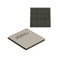
EP4SGX530HH35C2N Altera, EP4SGX530HH35C2N Datasheet - Page 664

EP4SGX530HH35C2N
Manufacturer Part Number
EP4SGX530HH35C2N
Description
IC STRATIX IV FPGA 530K 1152HBGA
Manufacturer
Altera
Series
Stratix® IV GXr
Datasheets
1.EP4SGX110DF29C3N.pdf
(80 pages)
2.EP4SGX110DF29C3N.pdf
(1154 pages)
3.EP4SGX110DF29C3N.pdf
(432 pages)
4.EP4SGX110DF29C3N.pdf
(22 pages)
5.EP4SGX110DF29C3N.pdf
(30 pages)
6.EP4SGX110DF29C3N.pdf
(72 pages)
7.EP4SGX530HH35C2N.pdf
(1145 pages)
Specifications of EP4SGX530HH35C2N
Number Of Logic Elements/cells
531200
Number Of Labs/clbs
21248
Total Ram Bits
27376
Number Of I /o
564
Voltage - Supply
0.87 V ~ 0.93 V
Mounting Type
Surface Mount
Operating Temperature
0°C ~ 85°C
Package / Case
1152-HBGA
Family Name
Stratix® IV
Number Of Logic Blocks/elements
531200
# Registers
424960
# I/os (max)
560
Process Technology
40nm
Operating Supply Voltage (typ)
900mV
Logic Cells
531200
Ram Bits
28033024
Operating Supply Voltage (min)
0.87V
Operating Supply Voltage (max)
0.93V
Operating Temp Range
0C to 85C
Operating Temperature Classification
Commercial
Mounting
Surface Mount
Pin Count
1152
Package Type
FCHBGA
Lead Free Status / RoHS Status
Lead free / RoHS Compliant
Number Of Gates
-
Lead Free Status / Rohs Status
Compliant
Available stocks
Company
Part Number
Manufacturer
Quantity
Price
- EP4SGX110DF29C3N PDF datasheet
- EP4SGX110DF29C3N PDF datasheet #2
- EP4SGX110DF29C3N PDF datasheet #3
- EP4SGX110DF29C3N PDF datasheet #4
- EP4SGX110DF29C3N PDF datasheet #5
- EP4SGX110DF29C3N PDF datasheet #6
- EP4SGX530HH35C2N PDF datasheet #7
- Current page: 664 of 1154
- Download datasheet (32Mb)
1–220
Table 1–76. Stratix IV GX and GT ALTGX Megafunction Ports: Dynamic Reconfiguration (Part 2 of 2)
Table 1–77. Stratix IV GX and GT ALTGX Megafunction Ports: PCIe Interface (Part 1 of 4)
Stratix IV Device Handbook Volume 2: Transceivers
reconfig_togxb
reconfig_fromgxb
powerdn
tx_
forcedispcompliance
tx_forceelecidle
rateswitch
Port Name
Port Name
Table 1–77
Output
Output
Input/
Input
Output
Input/
Input
Input
Input
Input
PCIe Interface (Available only in PCIe functional Mode)
lists the ALTGX megafunction PCIe interface ports.
Clock Domain
Asynchronous
Asynchronous
Clock Domain
Asynchronous
Asynchronous
Asynchronous
Asynchronous
signal
signal
signal
signal
signal
signal
From the dynamic reconfiguration controller.
To the dynamic reconfiguration controller.
PCIe power state control.
■
■
Force 8B/10B encoder to encode with a negative
running disparity.
■
■
Force transmitter buffer to PCIe electrical idle
signal levels.
■
■
PCIe rateswitch control.
■
■
Functionally equivalent to the powerdown[1:0]
signal defined in the PCIe specification revision
2.0.
The width of this signal is 2 bits and is encoded
as follows:
■
■
■
■
Functionally equivalent to the txcompliance
signal defined in PCIe specification revision 2.0.
Must be asserted high only when transmitting
the first byte of the PCIe compliance pattern to
force the 8B/10B encode with a negative running
disparity as required by the PCIe protocol.
Functionally equivalent to the txelecidle
signal defined in the PCIe specification revision
2.0.
Available in the Basic mode.
1’b0—Gen1 (2.5 Gbps)
1’b1—Gen2 (5 Gbps)
2'b00: P0—Normal Operation
2'b01: P0s—Low Recovery Time Latency,
Low Power State
2'b10: P1—Longer Recovery Time Latency,
Lower Power State
2'b11: P2—Lowest Power State
Chapter 1: Transceiver Architecture in Stratix IV Devices
Description
Description
February 2011 Altera Corporation
Transceiver Port Lists
Scope
Channel
Channel
Channel
Scope
Related parts for EP4SGX530HH35C2N
Image
Part Number
Description
Manufacturer
Datasheet
Request
R

Part Number:
Description:
CYCLONE II STARTER KIT EP2C20N
Manufacturer:
Altera
Datasheet:

Part Number:
Description:
CPLD, EP610 Family, ECMOS Process, 300 Gates, 16 Macro Cells, 16 Reg., 16 User I/Os, 5V Supply, 35 Speed Grade, 24DIP
Manufacturer:
Altera Corporation
Datasheet:

Part Number:
Description:
CPLD, EP610 Family, ECMOS Process, 300 Gates, 16 Macro Cells, 16 Reg., 16 User I/Os, 5V Supply, 15 Speed Grade, 24DIP
Manufacturer:
Altera Corporation
Datasheet:

Part Number:
Description:
Manufacturer:
Altera Corporation
Datasheet:

Part Number:
Description:
CPLD, EP610 Family, ECMOS Process, 300 Gates, 16 Macro Cells, 16 Reg., 16 User I/Os, 5V Supply, 30 Speed Grade, 24DIP
Manufacturer:
Altera Corporation
Datasheet:

Part Number:
Description:
High-performance, low-power erasable programmable logic devices with 8 macrocells, 10ns
Manufacturer:
Altera Corporation
Datasheet:

Part Number:
Description:
High-performance, low-power erasable programmable logic devices with 8 macrocells, 7ns
Manufacturer:
Altera Corporation
Datasheet:

Part Number:
Description:
Classic EPLD
Manufacturer:
Altera Corporation
Datasheet:

Part Number:
Description:
High-performance, low-power erasable programmable logic devices with 8 macrocells, 10ns
Manufacturer:
Altera Corporation
Datasheet:

Part Number:
Description:
Manufacturer:
Altera Corporation
Datasheet:

Part Number:
Description:
Manufacturer:
Altera Corporation
Datasheet:

Part Number:
Description:
Manufacturer:
Altera Corporation
Datasheet:

Part Number:
Description:
CPLD, EP610 Family, ECMOS Process, 300 Gates, 16 Macro Cells, 16 Reg., 16 User I/Os, 5V Supply, 25 Speed Grade, 24DIP
Manufacturer:
Altera Corporation
Datasheet:


