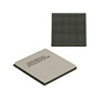
EP4SGX530HH35C2N Altera, EP4SGX530HH35C2N Datasheet - Page 218

EP4SGX530HH35C2N
Manufacturer Part Number
EP4SGX530HH35C2N
Description
IC STRATIX IV FPGA 530K 1152HBGA
Manufacturer
Altera
Series
Stratix® IV GXr
Datasheets
1.EP4SGX110DF29C3N.pdf
(80 pages)
2.EP4SGX110DF29C3N.pdf
(1154 pages)
3.EP4SGX110DF29C3N.pdf
(432 pages)
4.EP4SGX110DF29C3N.pdf
(22 pages)
5.EP4SGX110DF29C3N.pdf
(30 pages)
6.EP4SGX110DF29C3N.pdf
(72 pages)
7.EP4SGX530HH35C2N.pdf
(1145 pages)
Specifications of EP4SGX530HH35C2N
Number Of Logic Elements/cells
531200
Number Of Labs/clbs
21248
Total Ram Bits
27376
Number Of I /o
564
Voltage - Supply
0.87 V ~ 0.93 V
Mounting Type
Surface Mount
Operating Temperature
0°C ~ 85°C
Package / Case
1152-HBGA
Family Name
Stratix® IV
Number Of Logic Blocks/elements
531200
# Registers
424960
# I/os (max)
560
Process Technology
40nm
Operating Supply Voltage (typ)
900mV
Logic Cells
531200
Ram Bits
28033024
Operating Supply Voltage (min)
0.87V
Operating Supply Voltage (max)
0.93V
Operating Temp Range
0C to 85C
Operating Temperature Classification
Commercial
Mounting
Surface Mount
Pin Count
1152
Package Type
FCHBGA
Lead Free Status / RoHS Status
Lead free / RoHS Compliant
Number Of Gates
-
Lead Free Status / Rohs Status
Compliant
Available stocks
Company
Part Number
Manufacturer
Quantity
Price
- EP4SGX110DF29C3N PDF datasheet
- EP4SGX110DF29C3N PDF datasheet #2
- EP4SGX110DF29C3N PDF datasheet #3
- EP4SGX110DF29C3N PDF datasheet #4
- EP4SGX110DF29C3N PDF datasheet #5
- EP4SGX110DF29C3N PDF datasheet #6
- EP4SGX530HH35C2N PDF datasheet #7
- Current page: 218 of 1154
- Download datasheet (32Mb)
6–46
Figure 6–35. Mini-LVDS I/O Standard Termination
Note to
(1) The R
Design Considerations
Stratix IV Device Handbook Volume 1
Termination
Termination
On-Board
External
OCT
Figure
S
I/O Bank Restrictions
and R
6–35:
f
P
1
Transmitter
values are pending characterization.
Transmitter
Mini-LVDS
Stratix IV devices support the mini-LVDS output standard with data rates up to
340 Mbps using LVDS output buffer types. For transmitters, use two single-ended
output buffers with external one- or three-resistor networks, as shown in
The one-resistor topology is for data rates up to 200 Mbps. The three-resistor topology
is for data rates above 200 Mbps. The row I/O banks support mini-LVDS output using
true LVDS output buffers without an external resistor network.
A resistor network is required to attenuate the LVDS output voltage swing to meet the
mini-LVDS specifications. You can modify the three-resistor network values to reduce
power or improve noise margin. The resistor values chosen must satisfy
on page
Altera recommends that you perform additional simulations using IBIS models to
validate that custom resistor values meet the RSDS requirements.
For more information about the mini-LVDS I/O standard, see the mini-LVDS
Specification from the Texas Instruments website at www.ti.com.
Although Stratix IV devices feature various I/O capabilities for high-performance
and high-speed system designs, there are several other design considerations that
require your attention to ensure the success of your designs.
Each I/O bank can simultaneously support multiple I/O standards. The following
sections provide guidelines for mixing non-voltage-referenced and voltage-referenced
I/O standards in Stratix IV devices.
One-Resistor Network (mini-LVDS_E_1R)
≤1 inch
≤1 inch
6–45.
R
R
P
P
50 Ω
50 Ω
50 Ω
50 Ω
100 Ω
100 Ω
Stratix IV OCT
(Note 1)
Receiver
Receiver
Transmitter
Transmitter
Three-Resistor Network (mini-LVDS_E_3R)
Chapter 6: I/O Features in Stratix IV Devices
R S
R S
≤1 inch
≤
R S
R S
1 inch
R
P
R
P
February 2011 Altera Corporation
50 Ω
50 Ω
50 Ω
50 Ω
100 Ω
Design Considerations
100
Equation 6–1
Figure
Stratix IV OCT
Ω
Receiver
Receiver
6–35.
Related parts for EP4SGX530HH35C2N
Image
Part Number
Description
Manufacturer
Datasheet
Request
R

Part Number:
Description:
CYCLONE II STARTER KIT EP2C20N
Manufacturer:
Altera
Datasheet:

Part Number:
Description:
CPLD, EP610 Family, ECMOS Process, 300 Gates, 16 Macro Cells, 16 Reg., 16 User I/Os, 5V Supply, 35 Speed Grade, 24DIP
Manufacturer:
Altera Corporation
Datasheet:

Part Number:
Description:
CPLD, EP610 Family, ECMOS Process, 300 Gates, 16 Macro Cells, 16 Reg., 16 User I/Os, 5V Supply, 15 Speed Grade, 24DIP
Manufacturer:
Altera Corporation
Datasheet:

Part Number:
Description:
Manufacturer:
Altera Corporation
Datasheet:

Part Number:
Description:
CPLD, EP610 Family, ECMOS Process, 300 Gates, 16 Macro Cells, 16 Reg., 16 User I/Os, 5V Supply, 30 Speed Grade, 24DIP
Manufacturer:
Altera Corporation
Datasheet:

Part Number:
Description:
High-performance, low-power erasable programmable logic devices with 8 macrocells, 10ns
Manufacturer:
Altera Corporation
Datasheet:

Part Number:
Description:
High-performance, low-power erasable programmable logic devices with 8 macrocells, 7ns
Manufacturer:
Altera Corporation
Datasheet:

Part Number:
Description:
Classic EPLD
Manufacturer:
Altera Corporation
Datasheet:

Part Number:
Description:
High-performance, low-power erasable programmable logic devices with 8 macrocells, 10ns
Manufacturer:
Altera Corporation
Datasheet:

Part Number:
Description:
Manufacturer:
Altera Corporation
Datasheet:

Part Number:
Description:
Manufacturer:
Altera Corporation
Datasheet:

Part Number:
Description:
Manufacturer:
Altera Corporation
Datasheet:

Part Number:
Description:
CPLD, EP610 Family, ECMOS Process, 300 Gates, 16 Macro Cells, 16 Reg., 16 User I/Os, 5V Supply, 25 Speed Grade, 24DIP
Manufacturer:
Altera Corporation
Datasheet:


