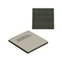
EP4SGX530HH35C2N Altera, EP4SGX530HH35C2N Datasheet - Page 469

EP4SGX530HH35C2N
Manufacturer Part Number
EP4SGX530HH35C2N
Description
IC STRATIX IV FPGA 530K 1152HBGA
Manufacturer
Altera
Series
Stratix® IV GXr
Datasheets
1.EP4SGX110DF29C3N.pdf
(80 pages)
2.EP4SGX110DF29C3N.pdf
(1154 pages)
3.EP4SGX110DF29C3N.pdf
(432 pages)
4.EP4SGX110DF29C3N.pdf
(22 pages)
5.EP4SGX110DF29C3N.pdf
(30 pages)
6.EP4SGX110DF29C3N.pdf
(72 pages)
7.EP4SGX530HH35C2N.pdf
(1145 pages)
Specifications of EP4SGX530HH35C2N
Number Of Logic Elements/cells
531200
Number Of Labs/clbs
21248
Total Ram Bits
27376
Number Of I /o
564
Voltage - Supply
0.87 V ~ 0.93 V
Mounting Type
Surface Mount
Operating Temperature
0°C ~ 85°C
Package / Case
1152-HBGA
Family Name
Stratix® IV
Number Of Logic Blocks/elements
531200
# Registers
424960
# I/os (max)
560
Process Technology
40nm
Operating Supply Voltage (typ)
900mV
Logic Cells
531200
Ram Bits
28033024
Operating Supply Voltage (min)
0.87V
Operating Supply Voltage (max)
0.93V
Operating Temp Range
0C to 85C
Operating Temperature Classification
Commercial
Mounting
Surface Mount
Pin Count
1152
Package Type
FCHBGA
Lead Free Status / RoHS Status
Lead free / RoHS Compliant
Number Of Gates
-
Lead Free Status / Rohs Status
Compliant
Available stocks
Company
Part Number
Manufacturer
Quantity
Price
- EP4SGX110DF29C3N PDF datasheet
- EP4SGX110DF29C3N PDF datasheet #2
- EP4SGX110DF29C3N PDF datasheet #3
- EP4SGX110DF29C3N PDF datasheet #4
- EP4SGX110DF29C3N PDF datasheet #5
- EP4SGX110DF29C3N PDF datasheet #6
- EP4SGX530HH35C2N PDF datasheet #7
- Current page: 469 of 1154
- Download datasheet (32Mb)
Chapter 1: Transceiver Architecture in Stratix IV Devices
Transceiver Block Architecture
Figure 1–20. 8B/10B Encoder Output During tx_digitalreset Assertion
February 2011 Altera Corporation
1
1
tx_digitalreset
dataout[9:0]
For example, depending on the current running disparity, the invalid code K24.1
(tx_datain = 8'h38 + tx_ctrl = 1'b1) can be encoded to 10'b0110001100 (0 × 18C),
which is equivalent to a D24.6+ (8'hD8 from the RD+ column). Altera recommends
that you do not assert tx_ctrlenable for unsupported 8-bit characters.
The tx_digitalreset signal resets the 8B/10B encoder. During reset, running
disparity and data registers are cleared. Also, the 8B/10B encoder outputs a K28.5
pattern from the RD- column continuously until tx_digitalreset is de-asserted. The
input data and control code from the FPGA fabric is ignored during the reset state.
After reset, the 8B/10B encoder starts with a negative disparity (RD-) and transmits
three K28.5 code groups for synchronization before it starts encoding and
transmitting the data on its output.
While tx_digitalreset is asserted, the downstream 8B/10B decoder that receives the
data might observe synchronization or disparity errors.
Figure 1–20
(tx_digitalreset is high), a K28.5- (K28.5 10-bit code group from the RD- column) is
sent continuously until tx_digitalreset is low. Due to some pipelining of the
transmitter channel PCS, some “don’t cares” (10'hxxx) are sent before the three
synchronizing K28.5 code groups. User data follows the third K28.5 code group.
In double-width mode, the 8B/10B encoder operates in a cascaded mode, as shown
on the right side of
and transmitted prior to the MSByte.
In double-width mode, the cascaded 8B/10B encoder generates two 10-bit code
groups from two 8-bit data and their respective control code identifiers.
shows the conversion format. The LSB shown in
clock
Reset Condition
Double-Width Mode
K28.5-
shows the reset behavior of the 8B/10B encoder. When in reset
K28.5-
Figure 1–20 on page
K28.5-
xxx
...
1–25. The LSByte of the input data is encoded
xxx
K28.5-
Figure 1–21
Stratix IV Device Handbook Volume 2: Transceivers
K28.5+
K28.5-
is transmitted first.
Dx.y+
Figure 1–21
1–25
Related parts for EP4SGX530HH35C2N
Image
Part Number
Description
Manufacturer
Datasheet
Request
R

Part Number:
Description:
CYCLONE II STARTER KIT EP2C20N
Manufacturer:
Altera
Datasheet:

Part Number:
Description:
CPLD, EP610 Family, ECMOS Process, 300 Gates, 16 Macro Cells, 16 Reg., 16 User I/Os, 5V Supply, 35 Speed Grade, 24DIP
Manufacturer:
Altera Corporation
Datasheet:

Part Number:
Description:
CPLD, EP610 Family, ECMOS Process, 300 Gates, 16 Macro Cells, 16 Reg., 16 User I/Os, 5V Supply, 15 Speed Grade, 24DIP
Manufacturer:
Altera Corporation
Datasheet:

Part Number:
Description:
Manufacturer:
Altera Corporation
Datasheet:

Part Number:
Description:
CPLD, EP610 Family, ECMOS Process, 300 Gates, 16 Macro Cells, 16 Reg., 16 User I/Os, 5V Supply, 30 Speed Grade, 24DIP
Manufacturer:
Altera Corporation
Datasheet:

Part Number:
Description:
High-performance, low-power erasable programmable logic devices with 8 macrocells, 10ns
Manufacturer:
Altera Corporation
Datasheet:

Part Number:
Description:
High-performance, low-power erasable programmable logic devices with 8 macrocells, 7ns
Manufacturer:
Altera Corporation
Datasheet:

Part Number:
Description:
Classic EPLD
Manufacturer:
Altera Corporation
Datasheet:

Part Number:
Description:
High-performance, low-power erasable programmable logic devices with 8 macrocells, 10ns
Manufacturer:
Altera Corporation
Datasheet:

Part Number:
Description:
Manufacturer:
Altera Corporation
Datasheet:

Part Number:
Description:
Manufacturer:
Altera Corporation
Datasheet:

Part Number:
Description:
Manufacturer:
Altera Corporation
Datasheet:

Part Number:
Description:
CPLD, EP610 Family, ECMOS Process, 300 Gates, 16 Macro Cells, 16 Reg., 16 User I/Os, 5V Supply, 25 Speed Grade, 24DIP
Manufacturer:
Altera Corporation
Datasheet:


