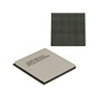
EP4SGX530HH35C2N Altera, EP4SGX530HH35C2N Datasheet - Page 23

EP4SGX530HH35C2N
Manufacturer Part Number
EP4SGX530HH35C2N
Description
IC STRATIX IV FPGA 530K 1152HBGA
Manufacturer
Altera
Series
Stratix® IV GXr
Datasheets
1.EP4SGX110DF29C3N.pdf
(80 pages)
2.EP4SGX110DF29C3N.pdf
(1154 pages)
3.EP4SGX110DF29C3N.pdf
(432 pages)
4.EP4SGX110DF29C3N.pdf
(22 pages)
5.EP4SGX110DF29C3N.pdf
(30 pages)
6.EP4SGX110DF29C3N.pdf
(72 pages)
7.EP4SGX530HH35C2N.pdf
(1145 pages)
Specifications of EP4SGX530HH35C2N
Number Of Logic Elements/cells
531200
Number Of Labs/clbs
21248
Total Ram Bits
27376
Number Of I /o
564
Voltage - Supply
0.87 V ~ 0.93 V
Mounting Type
Surface Mount
Operating Temperature
0°C ~ 85°C
Package / Case
1152-HBGA
Family Name
Stratix® IV
Number Of Logic Blocks/elements
531200
# Registers
424960
# I/os (max)
560
Process Technology
40nm
Operating Supply Voltage (typ)
900mV
Logic Cells
531200
Ram Bits
28033024
Operating Supply Voltage (min)
0.87V
Operating Supply Voltage (max)
0.93V
Operating Temp Range
0C to 85C
Operating Temperature Classification
Commercial
Mounting
Surface Mount
Pin Count
1152
Package Type
FCHBGA
Lead Free Status / RoHS Status
Lead free / RoHS Compliant
Number Of Gates
-
Lead Free Status / Rohs Status
Compliant
Available stocks
Company
Part Number
Manufacturer
Quantity
Price
- EP4SGX110DF29C3N PDF datasheet
- EP4SGX110DF29C3N PDF datasheet #2
- EP4SGX110DF29C3N PDF datasheet #3
- EP4SGX110DF29C3N PDF datasheet #4
- EP4SGX110DF29C3N PDF datasheet #5
- EP4SGX110DF29C3N PDF datasheet #6
- EP4SGX530HH35C2N PDF datasheet #7
- Current page: 23 of 1154
- Download datasheet (32Mb)
Chapter 1: Overview for the Stratix IV Device Family
Architecture Features
February 2011 Altera Corporation
PLLs
■
■
I/O Features
■
■
■
■
■
■
High-Speed Differential I/O with DPA and Soft-CDR
■
■
■
■
External Memory Interfaces
■
■
■
■
Three to 12 PLLs per device supporting spread-spectrum input tracking,
programmable bandwidth, clock switchover, dynamic reconfiguration, and delay
compensation
On-chip PLL power supply regulators to minimize noise coupling
Sixteen to 24 modular I/O banks per device with 24 to 48 I/Os per bank designed
and packaged for optimal simultaneous switching noise (SSN) performance and
migration capability
Support for a wide range of industry I/O standards, including single-ended
(LVTTL/CMOS/PCI/PCIX), differential (LVDS/mini-LVDS/RSDS),
voltage-referenced single-ended and differential (SSTL/HSTL Class I/II) I/O
standards
On-chip series (R
single-ended I/Os and on-chip differential (R
Programmable output drive strength, slew rate control, bus hold, and weak
pull-up capability for single-ended I/Os
User I/O:GND:V
interface
Programmable transmitter differential output voltage (V
high-speed LVDS I/O
Dedicated circuitry on the left and right sides of the device to support differential
links at data rates from 150 Mbps to 1.6 Gbps
Up to 98 differential SERDES in Stratix IV GX devices, up to 132 differential
SERDES in Stratix IV E devices, and up to 47 differential SERDES in Stratix IV GT
devices
DPA circuitry at the receiver automatically compensates for channel-to-channel
and channel-to-clock skew in source synchronous interfaces
Soft-CDR circuitry at the receiver allows implementation of asynchronous serial
interfaces with embedded clocks at up to 1.6 Gbps data rate (SGMII and GbE)
Support for existing and emerging memory interface standards such as DDR
SDRAM, DDR2 SDRAM, DDR3 SDRAM, QDRII SRAM, QDRII+ SRAM, and
RLDRAM II
DDR3 up to 1,067 Mbps/533 MHz
Programmable DQ group widths of 4 to 36 bits (includes parity bits)
Dynamic OCT, trace mismatch compensation, read-write leveling, and half-rate
register capabilities provide a robust external memory interface solution
S
CC
) and on-chip parallel (R
ratio of 8:1:1 to reduce loop inductance in the package—PCB
T
) termination with auto-calibration for
D
) termination for differential I/Os
Stratix IV Device Handbook Volume 1
OD
) and pre-emphasis for
1–9
Related parts for EP4SGX530HH35C2N
Image
Part Number
Description
Manufacturer
Datasheet
Request
R

Part Number:
Description:
CYCLONE II STARTER KIT EP2C20N
Manufacturer:
Altera
Datasheet:

Part Number:
Description:
CPLD, EP610 Family, ECMOS Process, 300 Gates, 16 Macro Cells, 16 Reg., 16 User I/Os, 5V Supply, 35 Speed Grade, 24DIP
Manufacturer:
Altera Corporation
Datasheet:

Part Number:
Description:
CPLD, EP610 Family, ECMOS Process, 300 Gates, 16 Macro Cells, 16 Reg., 16 User I/Os, 5V Supply, 15 Speed Grade, 24DIP
Manufacturer:
Altera Corporation
Datasheet:

Part Number:
Description:
Manufacturer:
Altera Corporation
Datasheet:

Part Number:
Description:
CPLD, EP610 Family, ECMOS Process, 300 Gates, 16 Macro Cells, 16 Reg., 16 User I/Os, 5V Supply, 30 Speed Grade, 24DIP
Manufacturer:
Altera Corporation
Datasheet:

Part Number:
Description:
High-performance, low-power erasable programmable logic devices with 8 macrocells, 10ns
Manufacturer:
Altera Corporation
Datasheet:

Part Number:
Description:
High-performance, low-power erasable programmable logic devices with 8 macrocells, 7ns
Manufacturer:
Altera Corporation
Datasheet:

Part Number:
Description:
Classic EPLD
Manufacturer:
Altera Corporation
Datasheet:

Part Number:
Description:
High-performance, low-power erasable programmable logic devices with 8 macrocells, 10ns
Manufacturer:
Altera Corporation
Datasheet:

Part Number:
Description:
Manufacturer:
Altera Corporation
Datasheet:

Part Number:
Description:
Manufacturer:
Altera Corporation
Datasheet:

Part Number:
Description:
Manufacturer:
Altera Corporation
Datasheet:

Part Number:
Description:
CPLD, EP610 Family, ECMOS Process, 300 Gates, 16 Macro Cells, 16 Reg., 16 User I/Os, 5V Supply, 25 Speed Grade, 24DIP
Manufacturer:
Altera Corporation
Datasheet:


