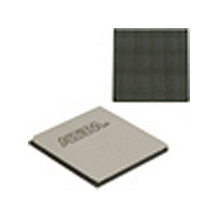
EP4SGX530HH35C2N Altera, EP4SGX530HH35C2N Datasheet - Page 486

EP4SGX530HH35C2N
Manufacturer Part Number
EP4SGX530HH35C2N
Description
IC STRATIX IV FPGA 530K 1152HBGA
Manufacturer
Altera
Series
Stratix® IV GXr
Datasheets
1.EP4SGX110DF29C3N.pdf
(80 pages)
2.EP4SGX110DF29C3N.pdf
(1154 pages)
3.EP4SGX110DF29C3N.pdf
(432 pages)
4.EP4SGX110DF29C3N.pdf
(22 pages)
5.EP4SGX110DF29C3N.pdf
(30 pages)
6.EP4SGX110DF29C3N.pdf
(72 pages)
7.EP4SGX530HH35C2N.pdf
(1145 pages)
Specifications of EP4SGX530HH35C2N
Number Of Logic Elements/cells
531200
Number Of Labs/clbs
21248
Total Ram Bits
27376
Number Of I /o
564
Voltage - Supply
0.87 V ~ 0.93 V
Mounting Type
Surface Mount
Operating Temperature
0°C ~ 85°C
Package / Case
1152-HBGA
Family Name
Stratix® IV
Number Of Logic Blocks/elements
531200
# Registers
424960
# I/os (max)
560
Process Technology
40nm
Operating Supply Voltage (typ)
900mV
Logic Cells
531200
Ram Bits
28033024
Operating Supply Voltage (min)
0.87V
Operating Supply Voltage (max)
0.93V
Operating Temp Range
0C to 85C
Operating Temperature Classification
Commercial
Mounting
Surface Mount
Pin Count
1152
Package Type
FCHBGA
Lead Free Status / RoHS Status
Lead free / RoHS Compliant
Number Of Gates
-
Lead Free Status / Rohs Status
Compliant
Available stocks
Company
Part Number
Manufacturer
Quantity
Price
- EP4SGX110DF29C3N PDF datasheet
- EP4SGX110DF29C3N PDF datasheet #2
- EP4SGX110DF29C3N PDF datasheet #3
- EP4SGX110DF29C3N PDF datasheet #4
- EP4SGX110DF29C3N PDF datasheet #5
- EP4SGX110DF29C3N PDF datasheet #6
- EP4SGX530HH35C2N PDF datasheet #7
- Current page: 486 of 1154
- Download datasheet (32Mb)
1–42
Stratix IV Device Handbook Volume 2: Transceivers
1
1
Programmable Differential On-Chip Termination
The Stratix IV GX and GT receiver buffers support optional differential OCT resistors
of 85, 100, 120, and 150 Ω . To select the desired receiver OCT resistor, make the
assignments shown in
Table 1–18. Stratix IV GX and GT Receiver On-Chip Termination Assignment Settings
The Stratix IV GX and GT receiver OCT resistors have calibration support to
compensate for process, voltage, and temperature variations. For more information
about OCT calibration support, refer to
The Stratix IV GX and GT receiver buffers have on-chip biasing circuitry to establish
the required V
that you can select in the ALTGX MegaWizard Plug-In Manager.
You must select 0.82 V as the receiver buffer V
buffer I/O standards:
■
■
■
■
You must select 1.1 V as the receiver buffer V
I/O standard.
On-chip biasing circuitry is effective only if you select on-chip receiver termination.
If you select external termination, you must implement off-chip biasing circuitry to
establish the V
A high-speed serial link can either be AC-coupled or DC-coupled, depending on the
serial protocol being implemented. Most of the serial protocols require links to be
AC-coupled, but protocols such as Common Electrical I/O (CEI) optionally allow DC
coupling.
Assignment Name
Stratix IV GX Available Values
Stratix IV GT Available Values
1.4-V PCML
1.5-V PCML
2.5-V PCML
LVPECL
Programmable V
Link Coupling for Stratix IV GX Devices
Assign To
CM
CM
at the receiver input. It supports V
at the receiver input buffer.
CM
Table 1–18
Input Termination
OCT 85 Ω , OCT 100 Ω , OCT 120 Ω, OCT 150 Ω , Off
OCT 85 Ω ,OCT 100 Ω , OCT 120 Ω , OCT 150 Ω , Off
in the Quartus II software Assignment Editor.
“Calibration Blocks” on page
rx_datain (Receiver Input Data Pins)
Chapter 1: Transceiver Architecture in Stratix IV Devices
CM
CM
for the LVDS receiver input buffer
for the following receiver input
CM
settings of 0.82 V and 1.1 V
February 2011 Altera Corporation
Transceiver Block Architecture
1–201.
Related parts for EP4SGX530HH35C2N
Image
Part Number
Description
Manufacturer
Datasheet
Request
R

Part Number:
Description:
CYCLONE II STARTER KIT EP2C20N
Manufacturer:
Altera
Datasheet:

Part Number:
Description:
CPLD, EP610 Family, ECMOS Process, 300 Gates, 16 Macro Cells, 16 Reg., 16 User I/Os, 5V Supply, 35 Speed Grade, 24DIP
Manufacturer:
Altera Corporation
Datasheet:

Part Number:
Description:
CPLD, EP610 Family, ECMOS Process, 300 Gates, 16 Macro Cells, 16 Reg., 16 User I/Os, 5V Supply, 15 Speed Grade, 24DIP
Manufacturer:
Altera Corporation
Datasheet:

Part Number:
Description:
Manufacturer:
Altera Corporation
Datasheet:

Part Number:
Description:
CPLD, EP610 Family, ECMOS Process, 300 Gates, 16 Macro Cells, 16 Reg., 16 User I/Os, 5V Supply, 30 Speed Grade, 24DIP
Manufacturer:
Altera Corporation
Datasheet:

Part Number:
Description:
High-performance, low-power erasable programmable logic devices with 8 macrocells, 10ns
Manufacturer:
Altera Corporation
Datasheet:

Part Number:
Description:
High-performance, low-power erasable programmable logic devices with 8 macrocells, 7ns
Manufacturer:
Altera Corporation
Datasheet:

Part Number:
Description:
Classic EPLD
Manufacturer:
Altera Corporation
Datasheet:

Part Number:
Description:
High-performance, low-power erasable programmable logic devices with 8 macrocells, 10ns
Manufacturer:
Altera Corporation
Datasheet:

Part Number:
Description:
Manufacturer:
Altera Corporation
Datasheet:

Part Number:
Description:
Manufacturer:
Altera Corporation
Datasheet:

Part Number:
Description:
Manufacturer:
Altera Corporation
Datasheet:

Part Number:
Description:
CPLD, EP610 Family, ECMOS Process, 300 Gates, 16 Macro Cells, 16 Reg., 16 User I/Os, 5V Supply, 25 Speed Grade, 24DIP
Manufacturer:
Altera Corporation
Datasheet:


