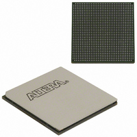
EP3SL150F1152C3N Altera, EP3SL150F1152C3N Datasheet - Page 191

EP3SL150F1152C3N
Manufacturer Part Number
EP3SL150F1152C3N
Description
IC STRATX III FPGA 150K 1152FBGA
Manufacturer
Altera
Series
Stratix® IIIr
Datasheets
1.EP3SL150F780C4N.pdf
(16 pages)
2.EP3SL150F780C4N.pdf
(332 pages)
3.EP3SL150F780C4N.pdf
(456 pages)
Specifications of EP3SL150F1152C3N
Number Of Logic Elements/cells
142500
Number Of Labs/clbs
5700
Total Ram Bits
6390
Number Of I /o
744
Voltage - Supply
0.86 V ~ 1.15 V
Mounting Type
Surface Mount
Operating Temperature
0°C ~ 85°C
Package / Case
1152-FBGA
For Use With
544-2568 - KIT DEVELOPMENT STRATIX III
Lead Free Status / RoHS Status
Lead free / RoHS Compliant
Number Of Gates
-
Other names
544-2408
EP3SL150F1152C3NES
EP3SL150F1152C3NES
Available stocks
Company
Part Number
Manufacturer
Quantity
Price
Company:
Part Number:
EP3SL150F1152C3N
Manufacturer:
ALTERA
Quantity:
490
- Current page: 191 of 456
- Download datasheet (7Mb)
Chapter 6: Clock Networks and PLLs in Stratix III Devices
PLLs in Stratix III Devices
Figure 6–40. PLL Reconfiguration Scan Chain
Notes to
(1) The Stratix III Left/Right PLLs support
(2) i = 6 or i = 9.
(3) This figure shows the corresponding scan register for the
© July 2010
scanclkena
configupdate
scandataout
counter is physically located after the VCO.
scandone
scandata
Figure
inclk
Altera Corporation
scanclk
6–40:
1
PLL Reconfiguration Hardware Implementation
The following PLL components are reconfigurable in real time:
■
■
■
■
■
Figure 6–40
their new settings into a serial shift-register chain or scan chain. Serial data is input to
the scan chain via the scandataport and shift registers are clocked by scanclk.
The maximum scanclk frequency is 100 MHz. Serial data is shifted through the scan
chain as long as the scanclkena signal stays asserted. After the last bit of data is
clocked, asserting the configupdate signal for at least one scanclk clock cycle
causes the PLL configuration bits to be synchronously updated with the data in the
scan registers.
The counter settings are updated synchronously to the clock frequency of the
individual counters. Therefore, all counters are not updated simultaneously.
from m counter
from n counter
/Ci (2)
Pre-scale counter (n)
Feedback counter (m)
Post-scale output counters (C0 – C9)
Post VCO Divider (K)
Dynamically adjust the charge-pump current (I
C) to facilitate reconfiguration of the PLL bandwidth
C0 - C6
/Ci-1
shows how PLL counter settings can be dynamically adjusted by shifting
counters
PFD
.
K
counter in between the scan registers for the charge pump and loop filter. The
/C2
LF/K/CP (3)
/C1
cp
/C0
) and loop-filter components (R,
VCO
Stratix III Device Handbook, Volume 1
/m
/n
6–43
K
Related parts for EP3SL150F1152C3N
Image
Part Number
Description
Manufacturer
Datasheet
Request
R

Part Number:
Description:
CYCLONE II STARTER KIT EP2C20N
Manufacturer:
Altera
Datasheet:

Part Number:
Description:
CPLD, EP610 Family, ECMOS Process, 300 Gates, 16 Macro Cells, 16 Reg., 16 User I/Os, 5V Supply, 35 Speed Grade, 24DIP
Manufacturer:
Altera Corporation
Datasheet:

Part Number:
Description:
CPLD, EP610 Family, ECMOS Process, 300 Gates, 16 Macro Cells, 16 Reg., 16 User I/Os, 5V Supply, 15 Speed Grade, 24DIP
Manufacturer:
Altera Corporation
Datasheet:

Part Number:
Description:
Manufacturer:
Altera Corporation
Datasheet:

Part Number:
Description:
CPLD, EP610 Family, ECMOS Process, 300 Gates, 16 Macro Cells, 16 Reg., 16 User I/Os, 5V Supply, 30 Speed Grade, 24DIP
Manufacturer:
Altera Corporation
Datasheet:

Part Number:
Description:
High-performance, low-power erasable programmable logic devices with 8 macrocells, 10ns
Manufacturer:
Altera Corporation
Datasheet:

Part Number:
Description:
High-performance, low-power erasable programmable logic devices with 8 macrocells, 7ns
Manufacturer:
Altera Corporation
Datasheet:

Part Number:
Description:
Classic EPLD
Manufacturer:
Altera Corporation
Datasheet:

Part Number:
Description:
High-performance, low-power erasable programmable logic devices with 8 macrocells, 10ns
Manufacturer:
Altera Corporation
Datasheet:

Part Number:
Description:
Manufacturer:
Altera Corporation
Datasheet:

Part Number:
Description:
Manufacturer:
Altera Corporation
Datasheet:

Part Number:
Description:
Manufacturer:
Altera Corporation
Datasheet:

Part Number:
Description:
CPLD, EP610 Family, ECMOS Process, 300 Gates, 16 Macro Cells, 16 Reg., 16 User I/Os, 5V Supply, 25 Speed Grade, 24DIP
Manufacturer:
Altera Corporation
Datasheet:


