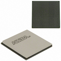
EP3SL150F1152C3N Altera, EP3SL150F1152C3N Datasheet - Page 291

EP3SL150F1152C3N
Manufacturer Part Number
EP3SL150F1152C3N
Description
IC STRATX III FPGA 150K 1152FBGA
Manufacturer
Altera
Series
Stratix® IIIr
Datasheets
1.EP3SL150F780C4N.pdf
(16 pages)
2.EP3SL150F780C4N.pdf
(332 pages)
3.EP3SL150F780C4N.pdf
(456 pages)
Specifications of EP3SL150F1152C3N
Number Of Logic Elements/cells
142500
Number Of Labs/clbs
5700
Total Ram Bits
6390
Number Of I /o
744
Voltage - Supply
0.86 V ~ 1.15 V
Mounting Type
Surface Mount
Operating Temperature
0°C ~ 85°C
Package / Case
1152-FBGA
For Use With
544-2568 - KIT DEVELOPMENT STRATIX III
Lead Free Status / RoHS Status
Lead free / RoHS Compliant
Number Of Gates
-
Other names
544-2408
EP3SL150F1152C3NES
EP3SL150F1152C3NES
Available stocks
Company
Part Number
Manufacturer
Quantity
Price
Company:
Part Number:
EP3SL150F1152C3N
Manufacturer:
ALTERA
Quantity:
490
- Current page: 291 of 456
- Download datasheet (7Mb)
Chapter 8: External Memory Interfaces in Stratix III Devices
Stratix III External Memory Interface Features
© March 2010 Altera Corporation
1
1
1
OCT
Stratix III devices feature dynamic calibrated OCT, in which series termination (OCT
R
parallel termination (OCT R
receiving signals. This feature complements the DDR3/DDR2 SDRAM on-die
termination (ODT), whereby memory termination is turned off when the memory is
sending data and turned on when receiving data. You can also use OCT for other
memory interfaces to improve signal integrity.
You cannot use the programmable drive strength and programmable slew rate
features when using OCT R
To use dynamic calibrated OCT, you must use the R
OCT calibration block. You can use one OCT calibration block to calibrate one type of
termination with the same V
calibration blocks to allow for different types of terminations throughout the device.
For more information, refer to
You have the option to use the OCT R
the OCT R
You can also use the R
DQS/DQ groups where the R
dynamic calibrated OCT. The R
DQS/DQ group on each side of the device.
Use the OCT RT/RS setting for uni-directional read and write data; use a dynamic
OCT setting for bi-directional data signals.
Programmable IOE Delay Chains
You can use programmable delay chains in the Stratix III I/O registers as deskewing
circuitry. Each pin can have a different input delay from the pin to input register or a
delay from the output register to the output pin to ensure that the bus has the same
delay going into or out of the FPGA. This feature helps read and write time margins
as it minimizes the uncertainties between signals in the bus.
Deskewing circuitry and programmable IOE delay chains are the same circuit.
Programmable Output Buffer Delay
In addition to allowing output buffer duty cycle adjustment, the programmable
output buffer delay chain allows you to adjust the delays between data bits in your
output bus to introduce or compensate channel-to-channel skew. Incorporating skew
to the output bus helps to minimize simultaneous switching events by enabling
smaller parts of the bus to switch simultaneously, instead of the whole bus. This
feature is particularly useful in DDR3 SDRAM interfaces where the memory system
clock delay can be much larger than the data and data clock/strobe delay. Use this
delay chain to add delay to the data and data clock/strobe to better match the
memory system clock delay.
S
) is turned on when driving signals and turned off when receiving signals, while the
T
feature is only available with calibration.
UP
and R
S
T
.
CCIO
) is turned off when driving signals and turned on when
UP
DN
“Dynamic OCT Control” on page
UP
and R
on the entire device. There are up to ten OCT
pins as DQ pins. However, you cannot use the ×4
and R
S
DN
feature with or without calibration. However,
DN
pins are located if you are planning to use
pins are located in the first and last ×4
UP
and R
Stratix III Device Handbook, Volume 1
DN
pins to calibrate the
8–33.
8–43
Related parts for EP3SL150F1152C3N
Image
Part Number
Description
Manufacturer
Datasheet
Request
R

Part Number:
Description:
CYCLONE II STARTER KIT EP2C20N
Manufacturer:
Altera
Datasheet:

Part Number:
Description:
CPLD, EP610 Family, ECMOS Process, 300 Gates, 16 Macro Cells, 16 Reg., 16 User I/Os, 5V Supply, 35 Speed Grade, 24DIP
Manufacturer:
Altera Corporation
Datasheet:

Part Number:
Description:
CPLD, EP610 Family, ECMOS Process, 300 Gates, 16 Macro Cells, 16 Reg., 16 User I/Os, 5V Supply, 15 Speed Grade, 24DIP
Manufacturer:
Altera Corporation
Datasheet:

Part Number:
Description:
Manufacturer:
Altera Corporation
Datasheet:

Part Number:
Description:
CPLD, EP610 Family, ECMOS Process, 300 Gates, 16 Macro Cells, 16 Reg., 16 User I/Os, 5V Supply, 30 Speed Grade, 24DIP
Manufacturer:
Altera Corporation
Datasheet:

Part Number:
Description:
High-performance, low-power erasable programmable logic devices with 8 macrocells, 10ns
Manufacturer:
Altera Corporation
Datasheet:

Part Number:
Description:
High-performance, low-power erasable programmable logic devices with 8 macrocells, 7ns
Manufacturer:
Altera Corporation
Datasheet:

Part Number:
Description:
Classic EPLD
Manufacturer:
Altera Corporation
Datasheet:

Part Number:
Description:
High-performance, low-power erasable programmable logic devices with 8 macrocells, 10ns
Manufacturer:
Altera Corporation
Datasheet:

Part Number:
Description:
Manufacturer:
Altera Corporation
Datasheet:

Part Number:
Description:
Manufacturer:
Altera Corporation
Datasheet:

Part Number:
Description:
Manufacturer:
Altera Corporation
Datasheet:

Part Number:
Description:
CPLD, EP610 Family, ECMOS Process, 300 Gates, 16 Macro Cells, 16 Reg., 16 User I/Os, 5V Supply, 25 Speed Grade, 24DIP
Manufacturer:
Altera Corporation
Datasheet:


