R5S72030W200FP Renesas Electronics America, R5S72030W200FP Datasheet - Page 1662
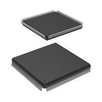
R5S72030W200FP
Manufacturer Part Number
R5S72030W200FP
Description
IC SUPERH MPU ROMLESS 240QFP
Manufacturer
Renesas Electronics America
Series
SuperH® SH7200r
Specifications of R5S72030W200FP
Core Processor
SH2A-FPU
Core Size
32-Bit
Speed
200MHz
Connectivity
CAN, I²C, SCI, SSI, SSU, USB
Peripherals
DMA, LCD, POR, PWM, WDT
Number Of I /o
82
Program Memory Type
ROMless
Ram Size
80K x 8
Voltage - Supply (vcc/vdd)
1.1 V ~ 3.6 V
Data Converters
A/D 8x10b; D/A 2x8b
Oscillator Type
Internal
Operating Temperature
-20°C ~ 85°C
Package / Case
240-QFP
For Use With
R0K572030S000BE - KIT DEV FOR SH7203HS0005KCU11H - EMULATOR E10A-USB H8S(X),SH2(A)
Lead Free Status / RoHS Status
Contains lead / RoHS non-compliant
Eeprom Size
-
Program Memory Size
-
Available stocks
Company
Part Number
Manufacturer
Quantity
Price
Company:

Part Number:
R5S72030W200FP
Manufacturer:
SAMSUNG
Quantity:
1 001
Company:
Part Number:
R5S72030W200FP
Manufacturer:
Renesas Electronics America
Quantity:
10 000


Rev. 3.00 Sep. 28, 2009 Page 1630 of 1650
REJ09B0313-0300
Item
20.4.5 Input Sampling
and A/D Conversion Time
Figure 20.5 A/D
Conversion Timing
20.7.8 Note on Usage in
Scan Mode and Multi
Mode
22.7 Usage Notes
23.2 Input/Output Pins
24.3 Register
Configuration
24.3.5 LCDC Start
Address Register for
Upper Display Data Fetch
(LDSARU)
Page
1037
1044
1096
1099
1236
1246
Revision (See Manual for Details)
Figure amended
Description amended
Starting conversion immediately after stopping scan mode or
multi mode can cause incorrect conversion results. To
continue with conversion in which cases, allow a duration
equivalent to the A/D conversion time for one channel to
elapse after clearing ADST to 0 before starting conversion
(by setting ADST to 1). (The A/D conversion time for one
channel differs depending on the peripheral register settings.)
Newly added
Description amended
•
Description amended
The LCDC includes the following registers. For description on
the address and processing status of these registers, refer to
section 34, List of Registers. The setting to LDSARU and
LDSARL are updated with the Vsync timing when the LCDC
is active.
Description amended
LDSARU sets the start address from which data is fetched by
the LCDC for display of the LCDC panel. When a DSTN
panel is used, this register specifies the fetch start address
for the upper side of the panel. The register setting is
updated with the Vsync timing when the LCDC is active.
Connect REFRIN to USBAPVCC through a 5.6 kΩ ± 20
% resistor
Pφ
Address
Write
signal
Input sampling
timing
ADF
(1)
(2)
t
D
t
SPL
t
CONV
Related parts for R5S72030W200FP
Image
Part Number
Description
Manufacturer
Datasheet
Request
R

Part Number:
Description:
KIT STARTER FOR M16C/29
Manufacturer:
Renesas Electronics America
Datasheet:

Part Number:
Description:
KIT STARTER FOR R8C/2D
Manufacturer:
Renesas Electronics America
Datasheet:

Part Number:
Description:
R0K33062P STARTER KIT
Manufacturer:
Renesas Electronics America
Datasheet:

Part Number:
Description:
KIT STARTER FOR R8C/23 E8A
Manufacturer:
Renesas Electronics America
Datasheet:

Part Number:
Description:
KIT STARTER FOR R8C/25
Manufacturer:
Renesas Electronics America
Datasheet:

Part Number:
Description:
KIT STARTER H8S2456 SHARPE DSPLY
Manufacturer:
Renesas Electronics America
Datasheet:

Part Number:
Description:
KIT STARTER FOR R8C38C
Manufacturer:
Renesas Electronics America
Datasheet:

Part Number:
Description:
KIT STARTER FOR R8C35C
Manufacturer:
Renesas Electronics America
Datasheet:

Part Number:
Description:
KIT STARTER FOR R8CL3AC+LCD APPS
Manufacturer:
Renesas Electronics America
Datasheet:
Part Number:
Description:
KIT STARTER FOR RX610
Manufacturer:
Renesas Electronics America
Datasheet:

Part Number:
Description:
KIT STARTER FOR R32C/118
Manufacturer:
Renesas Electronics America
Datasheet:

Part Number:
Description:
KIT DEV RSK-R8C/26-29
Manufacturer:
Renesas Electronics America
Datasheet:

Part Number:
Description:
KIT STARTER FOR SH7124
Manufacturer:
Renesas Electronics America
Datasheet:

Part Number:
Description:
KIT STARTER FOR H8SX/1622
Manufacturer:
Renesas Electronics America
Datasheet:

Part Number:
Description:
KIT DEV FOR SH7203
Manufacturer:
Renesas Electronics America
Datasheet: