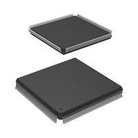
R5S72030W200FP Renesas Electronics America, R5S72030W200FP Datasheet - Page 858

R5S72030W200FP
Manufacturer Part Number
R5S72030W200FP
Description
IC SUPERH MPU ROMLESS 240QFP
Manufacturer
Renesas Electronics America
Series
SuperH® SH7200r
Specifications of R5S72030W200FP
Core Processor
SH2A-FPU
Core Size
32-Bit
Speed
200MHz
Connectivity
CAN, I²C, SCI, SSI, SSU, USB
Peripherals
DMA, LCD, POR, PWM, WDT
Number Of I /o
82
Program Memory Type
ROMless
Ram Size
80K x 8
Voltage - Supply (vcc/vdd)
1.1 V ~ 3.6 V
Data Converters
A/D 8x10b; D/A 2x8b
Oscillator Type
Internal
Operating Temperature
-20°C ~ 85°C
Package / Case
240-QFP
For Use With
R0K572030S000BE - KIT DEV FOR SH7203HS0005KCU11H - EMULATOR E10A-USB H8S(X),SH2(A)
Lead Free Status / RoHS Status
Contains lead / RoHS non-compliant
Eeprom Size
-
Program Memory Size
-
Available stocks
Company
Part Number
Manufacturer
Quantity
Price
Company:
Part Number:
R5S72030W200FP
Manufacturer:
SAMSUNG
Quantity:
1 001
Company:
Part Number:
R5S72030W200FP
Manufacturer:
Renesas Electronics America
Quantity:
10 000
- Current page: 858 of 1686
- Download datasheet (10Mb)
Section 16 Synchronous Serial Communication Unit (SSU)
(3)
Figure 16.15 shows an example of reception operation, and figure 16.16 shows a flowchart
example of data reception. When receiving data, the SSU operates as shown below.
After setting the RE bit in SSER to 1, the SSU starts data reception.
In master mode, the SSU outputs a transfer clock and receives data. In slave mode, when a transfer
clock is input to the SSCK pin, the SSU receives data in synchronization with the transfer clock.
When 1-frame data has been received, the RDRF bit in SSSR is set to 1 and the receive data is
stored in SSRDR. At this time, if the RIE bit is set to 1, an SSRXI interrupt is generated. The
RDRF bit is automatically cleared to 0 by reading SSRDR.
When the RDRF bit has been set to 1 at the 8th rising edge of the transfer clock, the ORER bit in
SSSR is set to 1. This indicates that an overrun error (SSERI) has occurred. At this time, data
reception is stopped. While the ORER bit in SSSR is set to 1, reception is not performed. To
resume the reception, clear the ORER bit to 0.
Rev. 3.00 Sep. 28, 2009 Page 826 of 1650
REJ09B0313-0300
User operation
LSI operation
Data Reception
RDRF
SSCK
SSO
Dummy-read SSRDR
Bit 0
Figure 16.15 Example of Reception Operation
(Clock Synchronous Communication Mode)
1 frame
Bit 7
SSRXI interrupt
generated
Bit 0
Read data from SSRDR
1 frame
SSRXI interrupt
generated
Bit 7
Bit 0
Read data from SSRDR
SSRXI interrupt
generated
Bit 7
Related parts for R5S72030W200FP
Image
Part Number
Description
Manufacturer
Datasheet
Request
R

Part Number:
Description:
KIT STARTER FOR M16C/29
Manufacturer:
Renesas Electronics America
Datasheet:

Part Number:
Description:
KIT STARTER FOR R8C/2D
Manufacturer:
Renesas Electronics America
Datasheet:

Part Number:
Description:
R0K33062P STARTER KIT
Manufacturer:
Renesas Electronics America
Datasheet:

Part Number:
Description:
KIT STARTER FOR R8C/23 E8A
Manufacturer:
Renesas Electronics America
Datasheet:

Part Number:
Description:
KIT STARTER FOR R8C/25
Manufacturer:
Renesas Electronics America
Datasheet:

Part Number:
Description:
KIT STARTER H8S2456 SHARPE DSPLY
Manufacturer:
Renesas Electronics America
Datasheet:

Part Number:
Description:
KIT STARTER FOR R8C38C
Manufacturer:
Renesas Electronics America
Datasheet:

Part Number:
Description:
KIT STARTER FOR R8C35C
Manufacturer:
Renesas Electronics America
Datasheet:

Part Number:
Description:
KIT STARTER FOR R8CL3AC+LCD APPS
Manufacturer:
Renesas Electronics America
Datasheet:

Part Number:
Description:
KIT STARTER FOR RX610
Manufacturer:
Renesas Electronics America
Datasheet:

Part Number:
Description:
KIT STARTER FOR R32C/118
Manufacturer:
Renesas Electronics America
Datasheet:

Part Number:
Description:
KIT DEV RSK-R8C/26-29
Manufacturer:
Renesas Electronics America
Datasheet:

Part Number:
Description:
KIT STARTER FOR SH7124
Manufacturer:
Renesas Electronics America
Datasheet:

Part Number:
Description:
KIT STARTER FOR H8SX/1622
Manufacturer:
Renesas Electronics America
Datasheet:

Part Number:
Description:
KIT DEV FOR SH7203
Manufacturer:
Renesas Electronics America
Datasheet:


