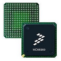
MC68EN360CAI25L Freescale Semiconductor, MC68EN360CAI25L Datasheet - Page 130

MC68EN360CAI25L
Manufacturer Part Number
MC68EN360CAI25L
Description
IC MPU QUICC 25MHZ 240-FQFP
Manufacturer
Freescale Semiconductor
Series
MC68000r
Datasheets
1.MC68EN302AG20BT.pdf
(8 pages)
2.MC68EN360VR25L.pdf
(14 pages)
3.MC68EN360VR25L.pdf
(2 pages)
4.MC68EN360CAI25L.pdf
(962 pages)
Specifications of MC68EN360CAI25L
Processor Type
M683xx 32-Bit
Speed
25MHz
Voltage
5V
Mounting Type
Surface Mount
Package / Case
240-FQFP
Core Size
32 Bit
Cpu Speed
25MHz
Embedded Interface Type
SCP, TDM
Digital Ic Case Style
FQFP
No. Of Pins
240
Supply Voltage Range
4.75V To 5.25V
Rohs Compliant
Yes
Family Name
M68xxx
Device Core
ColdFire
Device Core Size
32b
Frequency (max)
25MHz
Instruction Set Architecture
RISC
Supply Voltage 1 (typ)
5V
Operating Supply Voltage (max)
5.25V
Operating Supply Voltage (min)
4.75V
Operating Temp Range
-40C to 85C
Operating Temperature Classification
Industrial
Mounting
Surface Mount
Pin Count
240
Package Type
FQFP
Lead Free Status / RoHS Status
Lead free / RoHS Compliant
Features
-
Lead Free Status / Rohs Status
Compliant
Available stocks
Company
Part Number
Manufacturer
Quantity
Price
Company:
Part Number:
MC68EN360CAI25L
Manufacturer:
APLHA
Quantity:
12 000
Company:
Part Number:
MC68EN360CAI25L
Manufacturer:
Freescale Semiconductor
Quantity:
10 000
Part Number:
MC68EN360CAI25L
Manufacturer:
FREESCALE
Quantity:
20 000
- MC68EN302AG20BT PDF datasheet
- MC68EN360VR25L PDF datasheet #2
- MC68EN360VR25L PDF datasheet #3
- MC68EN360CAI25L PDF datasheet #4
- Current page: 130 of 962
- Download datasheet (4Mb)
Freescale Semiconductor, Inc.
Bus Operation
Once an external device receives the bus and asserts BGACK, it should negate BR. If BR
remains asserted after BGACK is asserted, the QUICC assumes that another device is
requesting the bus and prepares to issue another BG.
4.6.4 Bus Arbitration Control
The bus arbitration control unit in the QUICC is implemented with a finite state machine. As
discussed previously, all asynchronous inputs to the QUICC are internally synchronized in
a maximum of two cycles of the clock. As shown in Figure 4-37, input signals labeled R and
A are internally synchronized versions of BR and BGACK, respectively. The BG output is
labeled G, and the internal high-impedance control signal is labeled T. If T is true, the
address, data, and control buses are placed in the high-impedance state after the next rising
edge following the negation of AS and RMC. All signals are shown in positive logic (active
high), regardless of their true active voltage level. The state machine shown in Figure 4-37
does not have a state 1 or state 4.
State changes occur on the next rising edge of the clock after the internal signal is valid. The
BG signal transitions on the rising edge of the clock after a state is reached during which G
changes. The bus control signals (controlled by T) are driven by the QUICC immediately fol-
lowing a state change, when bus mastership is returned to the QUICC. State 0, in which G
and T are both negated, is the state of the bus arbiter while the QUICC is bus master. R and
A keep the arbiter in state 0 as long as they are both negated.
The QUICC does not allow arbitration of the external bus during the RMC sequence. For the
duration of this sequence, the QUICC ignores the BR input. If mastership of the bus is
required during an RMC operation, BERR must be used to abort the RMC sequence.
4-54
MC68360 USER’S MANUAL
For More Information On This Product,
Go to: www.freescale.com
Related parts for MC68EN360CAI25L
Image
Part Number
Description
Manufacturer
Datasheet
Request
R
Part Number:
Description:
Manufacturer:
Freescale Semiconductor, Inc
Datasheet:
Part Number:
Description:
Manufacturer:
Freescale Semiconductor, Inc
Datasheet:
Part Number:
Description:
Manufacturer:
Freescale Semiconductor, Inc
Datasheet:
Part Number:
Description:
Manufacturer:
Freescale Semiconductor, Inc
Datasheet:
Part Number:
Description:
Manufacturer:
Freescale Semiconductor, Inc
Datasheet:
Part Number:
Description:
Manufacturer:
Freescale Semiconductor, Inc
Datasheet:
Part Number:
Description:
Manufacturer:
Freescale Semiconductor, Inc
Datasheet:
Part Number:
Description:
Manufacturer:
Freescale Semiconductor, Inc
Datasheet:
Part Number:
Description:
Manufacturer:
Freescale Semiconductor, Inc
Datasheet:
Part Number:
Description:
Manufacturer:
Freescale Semiconductor, Inc
Datasheet:
Part Number:
Description:
Manufacturer:
Freescale Semiconductor, Inc
Datasheet:
Part Number:
Description:
Manufacturer:
Freescale Semiconductor, Inc
Datasheet:
Part Number:
Description:
Manufacturer:
Freescale Semiconductor, Inc
Datasheet:
Part Number:
Description:
Manufacturer:
Freescale Semiconductor, Inc
Datasheet:
Part Number:
Description:
Manufacturer:
Freescale Semiconductor, Inc
Datasheet:


