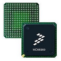
MC68EN360CAI25L Freescale Semiconductor, MC68EN360CAI25L Datasheet - Page 593

MC68EN360CAI25L
Manufacturer Part Number
MC68EN360CAI25L
Description
IC MPU QUICC 25MHZ 240-FQFP
Manufacturer
Freescale Semiconductor
Series
MC68000r
Datasheets
1.MC68EN302AG20BT.pdf
(8 pages)
2.MC68EN360VR25L.pdf
(14 pages)
3.MC68EN360VR25L.pdf
(2 pages)
4.MC68EN360CAI25L.pdf
(962 pages)
Specifications of MC68EN360CAI25L
Processor Type
M683xx 32-Bit
Speed
25MHz
Voltage
5V
Mounting Type
Surface Mount
Package / Case
240-FQFP
Core Size
32 Bit
Cpu Speed
25MHz
Embedded Interface Type
SCP, TDM
Digital Ic Case Style
FQFP
No. Of Pins
240
Supply Voltage Range
4.75V To 5.25V
Rohs Compliant
Yes
Family Name
M68xxx
Device Core
ColdFire
Device Core Size
32b
Frequency (max)
25MHz
Instruction Set Architecture
RISC
Supply Voltage 1 (typ)
5V
Operating Supply Voltage (max)
5.25V
Operating Supply Voltage (min)
4.75V
Operating Temp Range
-40C to 85C
Operating Temperature Classification
Industrial
Mounting
Surface Mount
Pin Count
240
Package Type
FQFP
Lead Free Status / RoHS Status
Lead free / RoHS Compliant
Features
-
Lead Free Status / Rohs Status
Compliant
Available stocks
Company
Part Number
Manufacturer
Quantity
Price
Company:
Part Number:
MC68EN360CAI25L
Manufacturer:
APLHA
Quantity:
12 000
Company:
Part Number:
MC68EN360CAI25L
Manufacturer:
Freescale Semiconductor
Quantity:
10 000
Part Number:
MC68EN360CAI25L
Manufacturer:
FREESCALE
Quantity:
20 000
- MC68EN302AG20BT PDF datasheet
- MC68EN360VR25L PDF datasheet #2
- MC68EN360VR25L PDF datasheet #3
- MC68EN360CAI25L PDF datasheet #4
- Current page: 593 of 962
- Download datasheet (4Mb)
Refer to Figure 7-73 for the SMC block diagram. The SMC receiver and transmitter are dou-
ble-buffered, as shown in the block diagram. This corresponds to an effective FIFO size
(latency) of two characters.
The receive data source for an SMC can be either the L1RXD pin if the SMC is connected
to a TDM channel of the SI, or the SMRXD pin if the SMC is connected to the NMSI. The
transmit data source can either be the L1TXD pin if the SMC is connected to a TDM, or the
SMTXD pin if the SMC is connected to the NMSI.
If the SMC is connected to a TDM, the SMC receive clock and SMC transmit clock can be
independent from each other as defined in the SI description. However, if the SMC is con-
nected to the NMSI, the SMC receive clock and SMC transmit clock must be connected to
a single clock source called SMCLK. SMCLK is an internal signal name for a clock that is
generated from the bank of clocks defined in the SI description. SMCLK may originate from
an external pin or one of the four internal baud rate generators. See 7.8.9 NMSI Configura-
tion for more details.
If the SMC is connected to a TDM, it derives its synchronization pulse from the TSA as
defined in the SI description. Otherwise, if the SMC is connected to the NMSI and the totally
transparent protocol is selected, the SMC may use the SMSYN pin as a synchronization pin
to determine when transmission and reception should begin. (The SMSYN pin is not used
in the SMC UART mode.)
T_ DATA_ REGISTER
TRANSMITTER
PAR TO SER
TX DATA
PERIPHERAL BUS
Freescale Semiconductor, Inc.
MODE _REGISTER
For More Information On This Product,
Figure 7-73. SMC Block Diagram
R_ DATA_ REGISTER
MC68360 USER’S MANUAL
SER TO PAR
Go to: www.freescale.com
RECEIVER
RX DATA
IMB
CONTROL
Serial Management Controllers (SMCs)
RX CLOCK
TX CLOCK
TO L1TXD IN SI OR SMTXD
FROM L1RXD IN SI OR SMRXD
SYNC
FROM SI OR SMSYN
FROM SI OR SMCLK
FROM SI OR SMCLK
Related parts for MC68EN360CAI25L
Image
Part Number
Description
Manufacturer
Datasheet
Request
R
Part Number:
Description:
Manufacturer:
Freescale Semiconductor, Inc
Datasheet:
Part Number:
Description:
Manufacturer:
Freescale Semiconductor, Inc
Datasheet:
Part Number:
Description:
Manufacturer:
Freescale Semiconductor, Inc
Datasheet:
Part Number:
Description:
Manufacturer:
Freescale Semiconductor, Inc
Datasheet:
Part Number:
Description:
Manufacturer:
Freescale Semiconductor, Inc
Datasheet:
Part Number:
Description:
Manufacturer:
Freescale Semiconductor, Inc
Datasheet:
Part Number:
Description:
Manufacturer:
Freescale Semiconductor, Inc
Datasheet:
Part Number:
Description:
Manufacturer:
Freescale Semiconductor, Inc
Datasheet:
Part Number:
Description:
Manufacturer:
Freescale Semiconductor, Inc
Datasheet:
Part Number:
Description:
Manufacturer:
Freescale Semiconductor, Inc
Datasheet:
Part Number:
Description:
Manufacturer:
Freescale Semiconductor, Inc
Datasheet:
Part Number:
Description:
Manufacturer:
Freescale Semiconductor, Inc
Datasheet:
Part Number:
Description:
Manufacturer:
Freescale Semiconductor, Inc
Datasheet:
Part Number:
Description:
Manufacturer:
Freescale Semiconductor, Inc
Datasheet:
Part Number:
Description:
Manufacturer:
Freescale Semiconductor, Inc
Datasheet:


