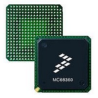
MC68EN360CAI25L Freescale Semiconductor, MC68EN360CAI25L Datasheet - Page 364

MC68EN360CAI25L
Manufacturer Part Number
MC68EN360CAI25L
Description
IC MPU QUICC 25MHZ 240-FQFP
Manufacturer
Freescale Semiconductor
Series
MC68000r
Datasheets
1.MC68EN302AG20BT.pdf
(8 pages)
2.MC68EN360VR25L.pdf
(14 pages)
3.MC68EN360VR25L.pdf
(2 pages)
4.MC68EN360CAI25L.pdf
(962 pages)
Specifications of MC68EN360CAI25L
Processor Type
M683xx 32-Bit
Speed
25MHz
Voltage
5V
Mounting Type
Surface Mount
Package / Case
240-FQFP
Core Size
32 Bit
Cpu Speed
25MHz
Embedded Interface Type
SCP, TDM
Digital Ic Case Style
FQFP
No. Of Pins
240
Supply Voltage Range
4.75V To 5.25V
Rohs Compliant
Yes
Family Name
M68xxx
Device Core
ColdFire
Device Core Size
32b
Frequency (max)
25MHz
Instruction Set Architecture
RISC
Supply Voltage 1 (typ)
5V
Operating Supply Voltage (max)
5.25V
Operating Supply Voltage (min)
4.75V
Operating Temp Range
-40C to 85C
Operating Temperature Classification
Industrial
Mounting
Surface Mount
Pin Count
240
Package Type
FQFP
Lead Free Status / RoHS Status
Lead free / RoHS Compliant
Features
-
Lead Free Status / Rohs Status
Compliant
Available stocks
Company
Part Number
Manufacturer
Quantity
Price
Company:
Part Number:
MC68EN360CAI25L
Manufacturer:
APLHA
Quantity:
12 000
Company:
Part Number:
MC68EN360CAI25L
Manufacturer:
Freescale Semiconductor
Quantity:
10 000
Part Number:
MC68EN360CAI25L
Manufacturer:
FREESCALE
Quantity:
20 000
- MC68EN302AG20BT PDF datasheet
- MC68EN360VR25L PDF datasheet #2
- MC68EN360VR25L PDF datasheet #3
- MC68EN360CAI25L PDF datasheet #4
- Current page: 364 of 962
- Download datasheet (4Mb)
IDMA Channels
interrupts, the IDMA may not be able to take its 128 clock allotment in a single burst. If, for
whatever reason, the IDMA is not able to take its full 128 clock allotment in a 1024 clock
cycle period, the IDMA is still only granted a 128 clock allotment in the next 1024 clock cycle
period.
7.6.4.4.3 External Burst Mode. For external devices requiring very high data transfer
rates, the external burst mode allows the IDMA to use all of the bus bandwidth to service the
device (see Figure 7-10). In the burst mode, the DREQx input to the IDMA is level-sensitive
and is sampled at falling edges of the clock to determine when a valid request is asserted
by the device. The device requests service by asserting DREQx and leaving it asserted. In
response, the IDMA begins to arbitrate for the system bus. If DREQx is negated prior to the
IDMA winning the bus, the IDMA will cease requesting the bus. If DREQx is negated long
enough for the IDMA to win the bus, cycles will continue as long as DREQx is asserted and
no higher priority bus master or interrupt occurs.
Each time the IDMA issues a bus cycle to either read or write the device, the IDMA will out-
put the DACKx signal. The device is either the source or destination of the transfers, as
7-40
(OUTPUT)
(OUTPUT)
(OUTPUT)
ECO = 1; PERIPHERAL IS READ.
NOTES:
ECO = 0; PERIPHERAL IS WRITTEN.
DSACKx
(INPUT)
DREQx
(INPUT)
DREQx
DACKx
CLKO1
DACKx
1. This example assumes dual address mode. In single address mode, the DREQx sample points would occur
2. This example assumes SRM = 1 in the CMR. If SRM = 0, DREQx would have to be asserted and negated one
(I/O)
S3 and S4) in all cycles shown above.
in every IDMA cycle.
clock earlier that what is shown to allow it to be internally synchronized by the IDMA before it is used.
Alternatively, the timing shown would be correct for the SRM = 0 case if a wait state were included (between
AS
S0
OTHER CYCLE
DREQ SAMPLED
LOW
DREQ SAMPLED
LOW
S2
S4
Freescale Semiconductor, Inc.
Figure 7-10. External Burst Requests;
For More Information On This Product,
S0
CONTINUE
BURST
IDMA READ
S2
MC68360 USER’S MANUAL
Go to: www.freescale.com
S4
CONTINUE
S0
BURST
IDMA WRITE
S2
S4
S0
IDMA READ
S2
STOP
BURST
S4
S0
IDMA WRITE
S2
STOP
BURST
S4
Related parts for MC68EN360CAI25L
Image
Part Number
Description
Manufacturer
Datasheet
Request
R
Part Number:
Description:
Manufacturer:
Freescale Semiconductor, Inc
Datasheet:
Part Number:
Description:
Manufacturer:
Freescale Semiconductor, Inc
Datasheet:
Part Number:
Description:
Manufacturer:
Freescale Semiconductor, Inc
Datasheet:
Part Number:
Description:
Manufacturer:
Freescale Semiconductor, Inc
Datasheet:
Part Number:
Description:
Manufacturer:
Freescale Semiconductor, Inc
Datasheet:
Part Number:
Description:
Manufacturer:
Freescale Semiconductor, Inc
Datasheet:
Part Number:
Description:
Manufacturer:
Freescale Semiconductor, Inc
Datasheet:
Part Number:
Description:
Manufacturer:
Freescale Semiconductor, Inc
Datasheet:
Part Number:
Description:
Manufacturer:
Freescale Semiconductor, Inc
Datasheet:
Part Number:
Description:
Manufacturer:
Freescale Semiconductor, Inc
Datasheet:
Part Number:
Description:
Manufacturer:
Freescale Semiconductor, Inc
Datasheet:
Part Number:
Description:
Manufacturer:
Freescale Semiconductor, Inc
Datasheet:
Part Number:
Description:
Manufacturer:
Freescale Semiconductor, Inc
Datasheet:
Part Number:
Description:
Manufacturer:
Freescale Semiconductor, Inc
Datasheet:
Part Number:
Description:
Manufacturer:
Freescale Semiconductor, Inc
Datasheet:


