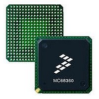
MC68EN360CAI25L Freescale Semiconductor, MC68EN360CAI25L Datasheet - Page 806

MC68EN360CAI25L
Manufacturer Part Number
MC68EN360CAI25L
Description
IC MPU QUICC 25MHZ 240-FQFP
Manufacturer
Freescale Semiconductor
Series
MC68000r
Datasheets
1.MC68EN302AG20BT.pdf
(8 pages)
2.MC68EN360VR25L.pdf
(14 pages)
3.MC68EN360VR25L.pdf
(2 pages)
4.MC68EN360CAI25L.pdf
(962 pages)
Specifications of MC68EN360CAI25L
Processor Type
M683xx 32-Bit
Speed
25MHz
Voltage
5V
Mounting Type
Surface Mount
Package / Case
240-FQFP
Core Size
32 Bit
Cpu Speed
25MHz
Embedded Interface Type
SCP, TDM
Digital Ic Case Style
FQFP
No. Of Pins
240
Supply Voltage Range
4.75V To 5.25V
Rohs Compliant
Yes
Family Name
M68xxx
Device Core
ColdFire
Device Core Size
32b
Frequency (max)
25MHz
Instruction Set Architecture
RISC
Supply Voltage 1 (typ)
5V
Operating Supply Voltage (max)
5.25V
Operating Supply Voltage (min)
4.75V
Operating Temp Range
-40C to 85C
Operating Temperature Classification
Industrial
Mounting
Surface Mount
Pin Count
240
Package Type
FQFP
Lead Free Status / RoHS Status
Lead free / RoHS Compliant
Features
-
Lead Free Status / Rohs Status
Compliant
Available stocks
Company
Part Number
Manufacturer
Quantity
Price
Company:
Part Number:
MC68EN360CAI25L
Manufacturer:
APLHA
Quantity:
12 000
Company:
Part Number:
MC68EN360CAI25L
Manufacturer:
Freescale Semiconductor
Quantity:
10 000
Part Number:
MC68EN360CAI25L
Manufacturer:
FREESCALE
Quantity:
20 000
- MC68EN302AG20BT PDF datasheet
- MC68EN360VR25L PDF datasheet #2
- MC68EN360VR25L PDF datasheet #3
- MC68EN360CAI25L PDF datasheet #4
- Current page: 806 of 962
- Download datasheet (4Mb)
Freescale Semiconductor, Inc.
Applications
This design also uses the RAS1 double-drive capability, whereby the RAS1DD signal is out-
put by the QUICC on the BCLRI pin to increase the effective drive capability of the RAS1
signal. The RAS1 line should be programmed to respond to a 4-Mbyte address space.
After power-on reset, the software must wait the required time before accessing the DRAM.
The required eight read cycles must then be performed either in software or by waiting for
the refresh controller to perform these accesses.
9.8.2.6 DRAM DEVICES. Figure 9-33 shows the interface to a standalone DRAM device. In
this case the MCM54260 256K
16 DRAM device is chosen. This allows a full 32-bit wide
DRAM solution using only two DRAM devices, with byte writes still supported using the
upper and lower CAS pins. Both the MC68EC030 and the QUICC can access the DRAM
array. The RAS1 line should be programmed to respond to a 1-Mbyte address space.
The address multiplexing scheme shown is the same as that for the DRAM SIMM. No parity
support is provided in this case. The RAS1DD signal is not used in this case, since only two
devices are supported.
After power-on reset, the software must wait the required time before accessing the DRAM,
and then perform the required eight read cycles, either in software or by waiting for the
refresh controller to perform these accesses.
9.8.3 Software Configuration
The following paragraphs discuss a number of key points for a software engineer desiring
to initialize the system. The only items discussed are those that are required to allow the pre-
viously discussed hardware configuration.
9.8.3.1 BASIC INITIALIZATION. The following register initializations are basic to all types
of applications.
The module base address register (MBAR) should be set as desired. However, the QUICC
8-Kbyte block should not overlap any memory array.
The module base address register enable (MBARE) should not be accessed.
In the module configuration register (MCR), ASTM and BSTM should be set to indicate syn-
chronous operation. SHEN1–SHEN0 should be cleared.
In the system protection control register (SYPCR), DBFE should be cleared. BME should be
set. If the software watchdog is used, the SWRI bit should be set.
The periodic interrupt control register (PICR) may be set as desired.
The port E pin assignment register (PEPAR) should be set to $51C0. This configures three
IOUTx lines to go out on the unused parity pins, the RAS1DD pin, WE lines instead of the
A31–A28 lines, the AMUX pin (assuming DRAM is used in the system; otherwise, the OE
function should be programmed), four CASx lines, CS7, and AVECO.
9-86
MC68360 USER’S MANUAL
For More Information On This Product,
Go to: www.freescale.com
Related parts for MC68EN360CAI25L
Image
Part Number
Description
Manufacturer
Datasheet
Request
R
Part Number:
Description:
Manufacturer:
Freescale Semiconductor, Inc
Datasheet:
Part Number:
Description:
Manufacturer:
Freescale Semiconductor, Inc
Datasheet:
Part Number:
Description:
Manufacturer:
Freescale Semiconductor, Inc
Datasheet:
Part Number:
Description:
Manufacturer:
Freescale Semiconductor, Inc
Datasheet:
Part Number:
Description:
Manufacturer:
Freescale Semiconductor, Inc
Datasheet:
Part Number:
Description:
Manufacturer:
Freescale Semiconductor, Inc
Datasheet:
Part Number:
Description:
Manufacturer:
Freescale Semiconductor, Inc
Datasheet:
Part Number:
Description:
Manufacturer:
Freescale Semiconductor, Inc
Datasheet:
Part Number:
Description:
Manufacturer:
Freescale Semiconductor, Inc
Datasheet:
Part Number:
Description:
Manufacturer:
Freescale Semiconductor, Inc
Datasheet:
Part Number:
Description:
Manufacturer:
Freescale Semiconductor, Inc
Datasheet:
Part Number:
Description:
Manufacturer:
Freescale Semiconductor, Inc
Datasheet:
Part Number:
Description:
Manufacturer:
Freescale Semiconductor, Inc
Datasheet:
Part Number:
Description:
Manufacturer:
Freescale Semiconductor, Inc
Datasheet:
Part Number:
Description:
Manufacturer:
Freescale Semiconductor, Inc
Datasheet:


