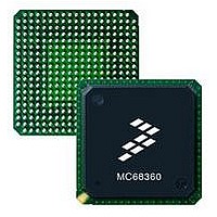
MC68EN360CAI25L Freescale Semiconductor, MC68EN360CAI25L Datasheet - Page 725

MC68EN360CAI25L
Manufacturer Part Number
MC68EN360CAI25L
Description
IC MPU QUICC 25MHZ 240-FQFP
Manufacturer
Freescale Semiconductor
Series
MC68000r
Datasheets
1.MC68EN302AG20BT.pdf
(8 pages)
2.MC68EN360VR25L.pdf
(14 pages)
3.MC68EN360VR25L.pdf
(2 pages)
4.MC68EN360CAI25L.pdf
(962 pages)
Specifications of MC68EN360CAI25L
Processor Type
M683xx 32-Bit
Speed
25MHz
Voltage
5V
Mounting Type
Surface Mount
Package / Case
240-FQFP
Core Size
32 Bit
Cpu Speed
25MHz
Embedded Interface Type
SCP, TDM
Digital Ic Case Style
FQFP
No. Of Pins
240
Supply Voltage Range
4.75V To 5.25V
Rohs Compliant
Yes
Family Name
M68xxx
Device Core
ColdFire
Device Core Size
32b
Frequency (max)
25MHz
Instruction Set Architecture
RISC
Supply Voltage 1 (typ)
5V
Operating Supply Voltage (max)
5.25V
Operating Supply Voltage (min)
4.75V
Operating Temp Range
-40C to 85C
Operating Temperature Classification
Industrial
Mounting
Surface Mount
Pin Count
240
Package Type
FQFP
Lead Free Status / RoHS Status
Lead free / RoHS Compliant
Features
-
Lead Free Status / Rohs Status
Compliant
Available stocks
Company
Part Number
Manufacturer
Quantity
Price
Company:
Part Number:
MC68EN360CAI25L
Manufacturer:
APLHA
Quantity:
12 000
Company:
Part Number:
MC68EN360CAI25L
Manufacturer:
Freescale Semiconductor
Quantity:
10 000
Part Number:
MC68EN360CAI25L
Manufacturer:
FREESCALE
Quantity:
20 000
- MC68EN302AG20BT PDF datasheet
- MC68EN360VR25L PDF datasheet #2
- MC68EN360VR25L PDF datasheet #3
- MC68EN360CAI25L PDF datasheet #4
- Current page: 725 of 962
- Download datasheet (4Mb)
9.1.2.2 REGULAR EPROM. Figure 9-2 shows the glueless interface to standard EPROM in
the system. In this case, an 8-bit boot EPROM is used. All accesses to the EPROM, even
word or long-word length, will be partitioned into multiple byte accesses to the EPROM.
The fact that the CONFIG2–CONFIG0 pins are pulled high causes these pins to default to
the 111 condition, selecting the CPU32+ core to be enabled, the CS0 pin to select a byte
port size, and the MBAR to be located in its normal address location. This is the most com-
monly used configuration for the CONFIGx pins. The pullups are used to allow for some of
the alternate functions of the CONFIGx pins to be used in later applications.
During initialization, CS0 should be programmed to respond to a 128-Kbyte area in this
design.
9.1.2.3 FLASH EPROM. Figure 9-3 shows the glueless interface to a flash EPROM device.
It is identical to the regular EPROM except that it allows for write operations as well. This
design assumes that the write operations are CE controlled, rather than WE controlled. Most
flash EPROM manufacturers now support this alternative timing method.
The fact that the CONFIGx pins are pulled high causes these pins to default to the 111 con-
dition, selecting the CPU32+ core to be enabled, the CS0 pin to select a byte port size, and
the MBAR to be located in its normal address location. This allows a byte-sized EPROM to
be used without any external glue logic.
Figure 9-2. Glueless Interface to Standard EPROM
Freescale Semiconductor, Inc.
D31–D24
CS0
For More Information On This Product,
SYSTEM BUS AND
QUICC-GENERATED SIGNALS
A16–A0
MC68360 USER’S MANUAL
Go to: www.freescale.com
+5V
DQ0
DQ1
DQ2
DQ3
DQ4
DQ5
DQ6
DQ7
OE
CE (ENABLE)
P
PORT SIZE
128K 8
EPROM
27C010
BYTE
A10
A12
A13
A14
A15
A16
A11
A8
A0
A2
A3
A4
A5
A6
A7
A9
A1
Applications
Related parts for MC68EN360CAI25L
Image
Part Number
Description
Manufacturer
Datasheet
Request
R
Part Number:
Description:
Manufacturer:
Freescale Semiconductor, Inc
Datasheet:
Part Number:
Description:
Manufacturer:
Freescale Semiconductor, Inc
Datasheet:
Part Number:
Description:
Manufacturer:
Freescale Semiconductor, Inc
Datasheet:
Part Number:
Description:
Manufacturer:
Freescale Semiconductor, Inc
Datasheet:
Part Number:
Description:
Manufacturer:
Freescale Semiconductor, Inc
Datasheet:
Part Number:
Description:
Manufacturer:
Freescale Semiconductor, Inc
Datasheet:
Part Number:
Description:
Manufacturer:
Freescale Semiconductor, Inc
Datasheet:
Part Number:
Description:
Manufacturer:
Freescale Semiconductor, Inc
Datasheet:
Part Number:
Description:
Manufacturer:
Freescale Semiconductor, Inc
Datasheet:
Part Number:
Description:
Manufacturer:
Freescale Semiconductor, Inc
Datasheet:
Part Number:
Description:
Manufacturer:
Freescale Semiconductor, Inc
Datasheet:
Part Number:
Description:
Manufacturer:
Freescale Semiconductor, Inc
Datasheet:
Part Number:
Description:
Manufacturer:
Freescale Semiconductor, Inc
Datasheet:
Part Number:
Description:
Manufacturer:
Freescale Semiconductor, Inc
Datasheet:
Part Number:
Description:
Manufacturer:
Freescale Semiconductor, Inc
Datasheet:


