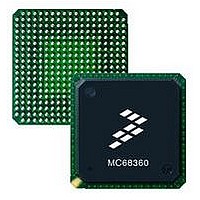
MC68EN360CAI25L Freescale Semiconductor, MC68EN360CAI25L Datasheet - Page 346

MC68EN360CAI25L
Manufacturer Part Number
MC68EN360CAI25L
Description
IC MPU QUICC 25MHZ 240-FQFP
Manufacturer
Freescale Semiconductor
Series
MC68000r
Datasheets
1.MC68EN302AG20BT.pdf
(8 pages)
2.MC68EN360VR25L.pdf
(14 pages)
3.MC68EN360VR25L.pdf
(2 pages)
4.MC68EN360CAI25L.pdf
(962 pages)
Specifications of MC68EN360CAI25L
Processor Type
M683xx 32-Bit
Speed
25MHz
Voltage
5V
Mounting Type
Surface Mount
Package / Case
240-FQFP
Core Size
32 Bit
Cpu Speed
25MHz
Embedded Interface Type
SCP, TDM
Digital Ic Case Style
FQFP
No. Of Pins
240
Supply Voltage Range
4.75V To 5.25V
Rohs Compliant
Yes
Family Name
M68xxx
Device Core
ColdFire
Device Core Size
32b
Frequency (max)
25MHz
Instruction Set Architecture
RISC
Supply Voltage 1 (typ)
5V
Operating Supply Voltage (max)
5.25V
Operating Supply Voltage (min)
4.75V
Operating Temp Range
-40C to 85C
Operating Temperature Classification
Industrial
Mounting
Surface Mount
Pin Count
240
Package Type
FQFP
Lead Free Status / RoHS Status
Lead free / RoHS Compliant
Features
-
Lead Free Status / Rohs Status
Compliant
Available stocks
Company
Part Number
Manufacturer
Quantity
Price
Company:
Part Number:
MC68EN360CAI25L
Manufacturer:
APLHA
Quantity:
12 000
Company:
Part Number:
MC68EN360CAI25L
Manufacturer:
Freescale Semiconductor
Quantity:
10 000
Part Number:
MC68EN360CAI25L
Manufacturer:
FREESCALE
Quantity:
20 000
- MC68EN302AG20BT PDF datasheet
- MC68EN360VR25L PDF datasheet #2
- MC68EN360VR25L PDF datasheet #3
- MC68EN360CAI25L PDF datasheet #4
- Current page: 346 of 962
- Download datasheet (4Mb)
Timers
ICLK—Input Clock Source for the Timer
GE—Gate Enable
7.5.2.4 TIMER REFERENCE REGISTERS (TRR1, TRR2, TRR3, TRR4). Each TRR is a
16-bit, memory-mapped, read-write register containing the reference value for the timeout.
TRR1–TRR4 are set to all ones by reset. The reference value is not reached until TCN incre-
ments to equal TRR.
7.5.2.5 TIMER CAPTURE REGISTERS (TCR1, TCR2, TCR3, TCR4). Each TCR is a 16-
bit register used to latch the value of the counter. TCR1–TCR4 appear as memory- mapped,
read-only registers to the user. TCR1–TCR4 are cleared by reset.
7.5.2.6 TIMER COUNTER (TCN1, TCN2, TCN3, TCN4). Each TCN is a 16-bit, memory-
mapped, read-write up-counter. A read cycle to TCN1–TCN4 yields the current value of the
timer, but does not affect the counting operation. A write cycle to TCN1–TCN4 sets the reg-
ister to the written value, causing its corresponding prescaler to be reset.
7.5.2.7 TIMER EVENT REGISTERS (TER1, TER2, TER3, TER4). Each TER is a 16-bit
register used to report events recognized by any of the timers. On recognition of an output
reference event, the timer sets the REF bit in the TER, regardless of the corresponding ORI
in the TMR. The capture event will be set only if enabled by the CE bits in the TMR. TER1–
TER4, which appear to the user as memory-mapped registers, may be read at any time.
A bit is reset by writing a one to that bit (writing a zero does not affect a bit’s value). More
than one bit may be reset at a time. Both bits must be reset before the timer will negate the
interrupt to the CPM interrupt controller. This register is cleared by reset.
Bits 15–2—Reserved
7-22
15
00 = Internally cascaded input.
01 = Internal general system clock.
10 = Internal general system clock divided by 16.
11 = Corresponding TIN pin: TIN1, TIN2, TIN3, or TIN4 (falling edge).
0 = The TGATE signal is ignored.
1 = The TGATE signal is used to control the timer.
14
For TMR1, the timer 1 input is the output of timer 2.
For TMR3, the timer 3 input is the output of timer 4.
For TMR2 and TMR4, this selection means no input clock is provided to the timer.
13
Write operation to this register while the timer is not running may
not update the register correctry. User should always use timer
refrence register to define desired count value.
12
11
Freescale Semiconductor, Inc.
For More Information On This Product,
10
MC68360 USER’S MANUAL
Go to: www.freescale.com
9
—
NOTE
8
7
6
5
4
3
2
REF
1
CAP
0
Related parts for MC68EN360CAI25L
Image
Part Number
Description
Manufacturer
Datasheet
Request
R
Part Number:
Description:
Manufacturer:
Freescale Semiconductor, Inc
Datasheet:
Part Number:
Description:
Manufacturer:
Freescale Semiconductor, Inc
Datasheet:
Part Number:
Description:
Manufacturer:
Freescale Semiconductor, Inc
Datasheet:
Part Number:
Description:
Manufacturer:
Freescale Semiconductor, Inc
Datasheet:
Part Number:
Description:
Manufacturer:
Freescale Semiconductor, Inc
Datasheet:
Part Number:
Description:
Manufacturer:
Freescale Semiconductor, Inc
Datasheet:
Part Number:
Description:
Manufacturer:
Freescale Semiconductor, Inc
Datasheet:
Part Number:
Description:
Manufacturer:
Freescale Semiconductor, Inc
Datasheet:
Part Number:
Description:
Manufacturer:
Freescale Semiconductor, Inc
Datasheet:
Part Number:
Description:
Manufacturer:
Freescale Semiconductor, Inc
Datasheet:
Part Number:
Description:
Manufacturer:
Freescale Semiconductor, Inc
Datasheet:
Part Number:
Description:
Manufacturer:
Freescale Semiconductor, Inc
Datasheet:
Part Number:
Description:
Manufacturer:
Freescale Semiconductor, Inc
Datasheet:
Part Number:
Description:
Manufacturer:
Freescale Semiconductor, Inc
Datasheet:
Part Number:
Description:
Manufacturer:
Freescale Semiconductor, Inc
Datasheet:


