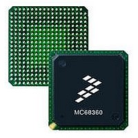
MC68EN360CAI25L Freescale Semiconductor, MC68EN360CAI25L Datasheet - Page 274

MC68EN360CAI25L
Manufacturer Part Number
MC68EN360CAI25L
Description
IC MPU QUICC 25MHZ 240-FQFP
Manufacturer
Freescale Semiconductor
Series
MC68000r
Datasheets
1.MC68EN302AG20BT.pdf
(8 pages)
2.MC68EN360VR25L.pdf
(14 pages)
3.MC68EN360VR25L.pdf
(2 pages)
4.MC68EN360CAI25L.pdf
(962 pages)
Specifications of MC68EN360CAI25L
Processor Type
M683xx 32-Bit
Speed
25MHz
Voltage
5V
Mounting Type
Surface Mount
Package / Case
240-FQFP
Core Size
32 Bit
Cpu Speed
25MHz
Embedded Interface Type
SCP, TDM
Digital Ic Case Style
FQFP
No. Of Pins
240
Supply Voltage Range
4.75V To 5.25V
Rohs Compliant
Yes
Family Name
M68xxx
Device Core
ColdFire
Device Core Size
32b
Frequency (max)
25MHz
Instruction Set Architecture
RISC
Supply Voltage 1 (typ)
5V
Operating Supply Voltage (max)
5.25V
Operating Supply Voltage (min)
4.75V
Operating Temp Range
-40C to 85C
Operating Temperature Classification
Industrial
Mounting
Surface Mount
Pin Count
240
Package Type
FQFP
Lead Free Status / RoHS Status
Lead free / RoHS Compliant
Features
-
Lead Free Status / Rohs Status
Compliant
Available stocks
Company
Part Number
Manufacturer
Quantity
Price
Company:
Part Number:
MC68EN360CAI25L
Manufacturer:
APLHA
Quantity:
12 000
Company:
Part Number:
MC68EN360CAI25L
Manufacturer:
Freescale Semiconductor
Quantity:
10 000
Part Number:
MC68EN360CAI25L
Manufacturer:
FREESCALE
Quantity:
20 000
- MC68EN302AG20BT PDF datasheet
- MC68EN360VR25L PDF datasheet #2
- MC68EN360VR25L PDF datasheet #3
- MC68EN360CAI25L PDF datasheet #4
- Current page: 274 of 962
- Download datasheet (4Mb)
System Integration Module (SIM60)
BR040ID2–BR040ID0—Bus Request MC68040 Arbitration ID
Bits 28–17—Reserved
BSTM—Bus Synchronous Timing Mode
6-30
ASTM
31
15
These bits contain the arbitration priority level for the MC68040 BR signal when the
QUICC is in MC68040 companion mode; otherwise, this value is ignored. The MC68040
BR signal in companion mode) is reflected on the IMB with the bus arbitration level corre-
sponding to these bits. This method gives the user a choice of where to place the arbitra-
tion level of the MC68040 (and other external masters in this system) relative to the IDMA,
SDMA, or DRAM refresh cycles generated by the QIUCC.
This bit determines whether the EBI will synchronize the AS and DS bus signals used for
an external master’s access into the QUICC peripherals and for CS and RAS generation
by the QUICC. The synchronization will add a one-clock delay to the RAS/CS assertion
for an external master. The MC68EC040 signals must always be synchronized to the
QUICC clock, regardless of the setting of this bit. See 6.10 Memory Controller for recom-
mendations on the setting of BSTM in certain situations.
BR040ID2–BR040ID0
0
0
0 = Asynchronous timing on the bus signals may be used. The bus signals are syn-
1 = Synchronous timing on the bus signals must be used. The bus control signals will
30
14
FRZ1–FRZ0
0
1
chronized internally by the QUICC and do not have to meet any timings relative to
the system clock.
not be synchronized internally and therefore must meet the system clock setup and
hold timings.
29
13
In a typical configuration, the user would program this value to a
3 to give the MC68040 priority over the IDMAs, but not over the
SDMAs and the DRAM refresh cycle. If the SDMAs, however,
are not of extremely high priority, the user may choose this value
to be 5. User should never program this field to be 7.
BCLRI, Address, Data, DSACK, BERR, HALT, RESETH, and
RESETS are always asynchronous.
0
1
BCLROID2–BCLROID0
28
12
—
0
1
27
11
—
Freescale Semiconductor, Inc.
0
1
For More Information On This Product,
26
10
—
0
1
MC68360 USER’S MANUAL
Go to: www.freescale.com
SHEN1–SHEN0
25
—
0
0
9
24
—
NOTE
NOTE
0
8
0
SUPV
23
—
0
7
1
BCLRISM2–BCLRISM0 or
22
—
0
6
1
BCLRIID2–BCLRIID0
21
—
0
5
1
20
—
0
4
1
19
—
0
3
1
IARB3–IARB0
18
—
0
2
1
17
—
0
1
1
BSTM
16
0
0
1
Related parts for MC68EN360CAI25L
Image
Part Number
Description
Manufacturer
Datasheet
Request
R
Part Number:
Description:
Manufacturer:
Freescale Semiconductor, Inc
Datasheet:
Part Number:
Description:
Manufacturer:
Freescale Semiconductor, Inc
Datasheet:
Part Number:
Description:
Manufacturer:
Freescale Semiconductor, Inc
Datasheet:
Part Number:
Description:
Manufacturer:
Freescale Semiconductor, Inc
Datasheet:
Part Number:
Description:
Manufacturer:
Freescale Semiconductor, Inc
Datasheet:
Part Number:
Description:
Manufacturer:
Freescale Semiconductor, Inc
Datasheet:
Part Number:
Description:
Manufacturer:
Freescale Semiconductor, Inc
Datasheet:
Part Number:
Description:
Manufacturer:
Freescale Semiconductor, Inc
Datasheet:
Part Number:
Description:
Manufacturer:
Freescale Semiconductor, Inc
Datasheet:
Part Number:
Description:
Manufacturer:
Freescale Semiconductor, Inc
Datasheet:
Part Number:
Description:
Manufacturer:
Freescale Semiconductor, Inc
Datasheet:
Part Number:
Description:
Manufacturer:
Freescale Semiconductor, Inc
Datasheet:
Part Number:
Description:
Manufacturer:
Freescale Semiconductor, Inc
Datasheet:
Part Number:
Description:
Manufacturer:
Freescale Semiconductor, Inc
Datasheet:
Part Number:
Description:
Manufacturer:
Freescale Semiconductor, Inc
Datasheet:


